Stripline Impedance Calculator
Model a copper trace fully embedded in dielectric between two reference planes. Enter trace width, plane-to-plane spacing, copper weight and dielectric constant to get characteristic impedance Z0 from the IPC-2141 stripline equation, plus propagation delay, capacitance and inductance per inch. Because the trace is buried, the effective permittivity equals the bulk Er, and both symmetric and offset builds are supported.
🧱Stripline Geometry Type
🎯Real Stackup Presets
📝Trace and Stackup Inputs
Finished copper width of the signal trace.
Total dielectric height between the two reference planes.
1 oz copper is about 1.378 mils thick.
Enter oz weight or mils to match the unit chosen above.
Bulk relative permittivity of the laminate. FR4 is near 4.2.
Distance the trace sits away from the mid-plane in offset mode.
Routed length used for the total propagation delay.
Controls rounding on every result card.
🔢Formula Snapshot
⚙Formula Breakdown
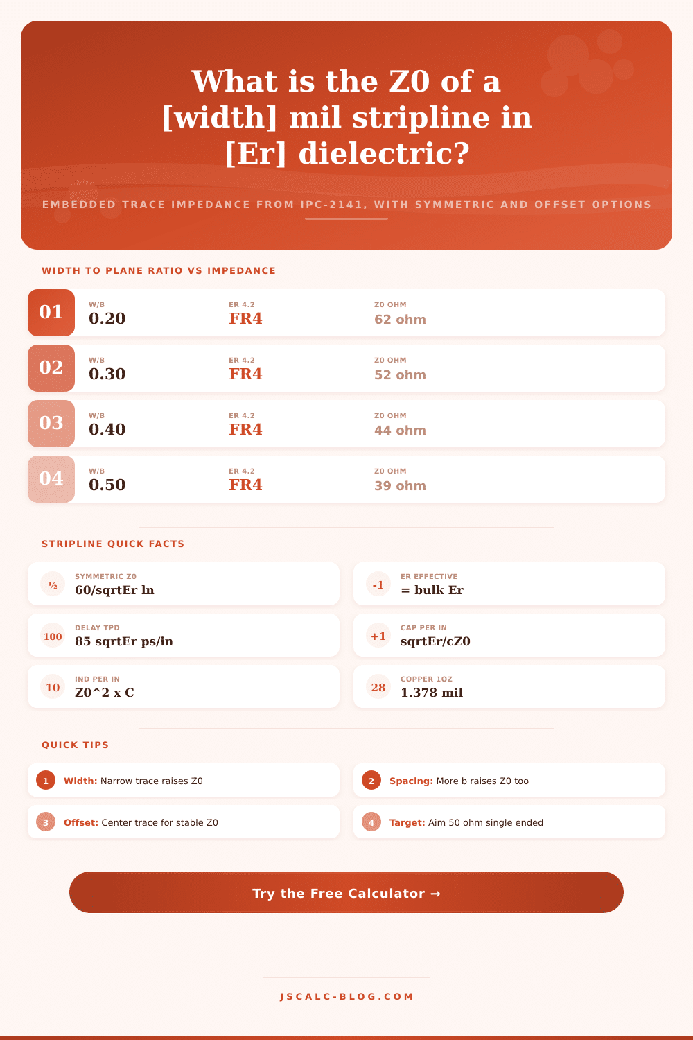
📋Width to Impedance for FR4
| Trace Width w | Spacing b | w/b Ratio | Approx Z0 (Er 4.2) |
|---|---|---|---|
| 4 mil | 20 mil | 0.20 | 62 ohm |
| 6 mil | 20 mil | 0.30 | 52 ohm |
| 8 mil | 20 mil | 0.40 | 44 ohm |
| 10 mil | 20 mil | 0.50 | 39 ohm |
| 12 mil | 20 mil | 0.60 | 34 ohm |
| 14 mil | 20 mil | 0.70 | 31 ohm |
| 16 mil | 20 mil | 0.80 | 28 ohm |
| 5 mil | 14 mil | 0.36 | 47 ohm |
📊Common Laminate Dielectric Constants
| Material | Er (approx) | tpd ps/in | Typical Use |
|---|---|---|---|
| FR4 standard | 4.2 | 174 ps/in | General digital boards |
| FR4 high Tg | 4.4 | 178 ps/in | Lead free assembly |
| Megtron 6 | 3.4 | 157 ps/in | High speed low loss |
| Isola 370HR | 4.0 | 170 ps/in | Cost aware high speed |
| Rogers 4350B | 3.48 | 159 ps/in | RF and microwave |
| Rogers 3003 | 3.0 | 147 ps/in | Millimeter wave |
| PTFE glass | 2.2 | 126 ps/in | Low loss RF stripline |
📏Copper Weight to Thickness
| Copper Weight | Thickness (mils) | Thickness (um) | Note |
|---|---|---|---|
| 0.5 oz | 0.689 mil | 17.5 um | Fine line inner layers |
| 1 oz | 1.378 mil | 35 um | Most common signal layer |
| 1.5 oz | 2.067 mil | 52.5 um | Higher current traces |
| 2 oz | 2.756 mil | 70 um | Power and heavy copper |
| 3 oz | 4.134 mil | 105 um | Bus bars and planes |
| 4 oz | 5.512 mil | 140 um | High current power |
🗃Stripline Impedance Comparison Grid
| Width w | Spacing b | w/b | Er 4.2 Z0 | Er 3.5 Z0 | Er 3.0 Z0 |
|---|---|---|---|---|---|
| 4 mil | 20 mil | 0.20 | 62 ohm | 68 ohm | 73 ohm |
| 5 mil | 20 mil | 0.25 | 56 ohm | 62 ohm | 67 ohm |
| 6 mil | 20 mil | 0.30 | 52 ohm | 57 ohm | 61 ohm |
| 8 mil | 20 mil | 0.40 | 44 ohm | 48 ohm | 52 ohm |
| 10 mil | 20 mil | 0.50 | 39 ohm | 42 ohm | 46 ohm |
| 5 mil | 14 mil | 0.36 | 47 ohm | 52 ohm | 56 ohm |
| 4 mil | 12 mil | 0.33 | 50 ohm | 55 ohm | 59 ohm |
| 6 mil | 24 mil | 0.25 | 56 ohm | 62 ohm | 67 ohm |
| 3 mil | 10 mil | 0.30 | 52 ohm | 57 ohm | 61 ohm |
| 8 mil | 30 mil | 0.27 | 54 ohm | 60 ohm | 64 ohm |
💡Stripline Design Tips
You trusted the trace width and never checked its thickness, you assumed the dielectric was uniform when it wasn’t… Something that passes signal integrity test fails to look right in the layout editor.
A stripline is a trace buried within laminate sandwiched between two ground planes. Because the trace is completely enclosed, the electric field stays inside the material instead of spreading into air. Striplines are therefore stable and predictable with an effective permittivity equal to bulk dielectric constant. It’s easier mathematically than microstrip calculations as long as you pay attention to variables that matter.
How to Use the Stripline Calculator
For this example we are using the IPC-2141 equation which can be found on this page. Simply fill in fields with your dimensions, material properties and let the calculator perform unit conversion and natural log calculations. Knowing how each input work is important.
The trace width is an easy one; the narrower you make it the higher the impedance. The thickness of copper works quietly here as well. Thicker copper provide a larger cross section for current to flow, which results in lower impedance. Most folks don’t think about this unless they run into trouble with their tolerance budget. However, the calculator takes that into account (in mils) and converts it to ounces for you, so you don’t have to keep up with all the conversions.
Another mistake involves offset, which is caused by manufacturing tolerances that move layers around and prevent actual trace stackup from being perfectly centered. As a trace comes nearer one of the planes it couples stronger with reference, lowering impedance. You can model the offset in the tool by entering an offset distance. If it’s a small amount, it may alter Z0 by a few ohms; but a big shift could wreck your match completely. For stability, it’s always best to keep things centered. If your panelizer has forced you to set an offset, tighten your width tolerance instead to compensate. People often miss this until they see the yield drop.
All others follow the material’s electrical property (Er) because that number describe the ability of the material to transport signal. For example, FR4 has an Er around 4.2 while high speed laminates such as Megtron approach 3.4. The lower the Er, the higher the impedance given the same geometry. Likewise, the lower Er allow for the signal to propagate faster. Propagation delay changes by the square root of permittivity which is why the calculator use Er directly in the delay equation. That is not a linear relationship, so small differences in material selection lead to huge variations in your timing budget. A 0.1 change in Er at long trace lengths can result in picoseconds of skew if you’re routing DDR or PCIe. Those picoseconds accumulates with increasing distance.
These values allow you to model transmission line behavior without pulling out your textbook; you get propagation delay, capacitance per inch, inductance per inch and yes, impedance too. You will note that capacitance decreases as Z0 increases, and increases with Er. Inductance follow from the ratio of Z0 squared to capacitance. Combined with their velocity factor, these form basis for characteristic impedance. Looking at C and L separately can help find where problem is if there are reflections. The cause could be a geometric mismatch or an oddity in the dielectric itself.
The nice part about it is you can save time by loading common specs such as 100 ohm differential legs or 50 ohm FR4 in a preset. Then mess around with width/spacing until you get your spec exactly right. If your calculation is far from what the table estimates, double-check your units. The quickest way to get nonsense numbers is to mix inches and mils. They’ve got some reference tables on the page to see how varying geometry and material changes Z0. These are quick lookups that let you check your sanity.
The “magic” of stripline isn’t found in formulas but in discipline. Double check your copper weight and laminate thickness against the fab before proceeding. Center your traces when you can. The calculator handles the math, but it could of not fix a poorly defined stackup. Do the geometry right then have the math confirm your gut feel. Treat a buried trace as a delicate structure; keep it consistent and centered, and it will be reliable. What appears to be a simple line in CAD is actualy a carefully crafted structure that conceals itself within plastic.