Microstrip Impedance Calculator
Model a single surface microstrip trace with the IPC-2141 equations. Enter trace width, dielectric height, copper weight, dielectric constant, length and frequency to get characteristic impedance Z0, the effective dielectric constant, propagation delay, and the capacitance and inductance per inch that set signal behavior on the line.
📡Real Microstrip Presets
📏Trace and Stackup Inputs
Conductor width of the top copper trace.
Substrate thickness between trace and ground plane.
1 oz equals 1.378 mils of copper thickness t.
Relative permittivity of the substrate, 4.3 for FR4.
Routed length, used for total delay and total L and C.
Signal frequency, used for the quarter-wave reference.
Design goal, compared to the computed Z0.
Controls rounding on every result card.
🔢Formula Snapshot
📡Trace Width to Impedance on FR4
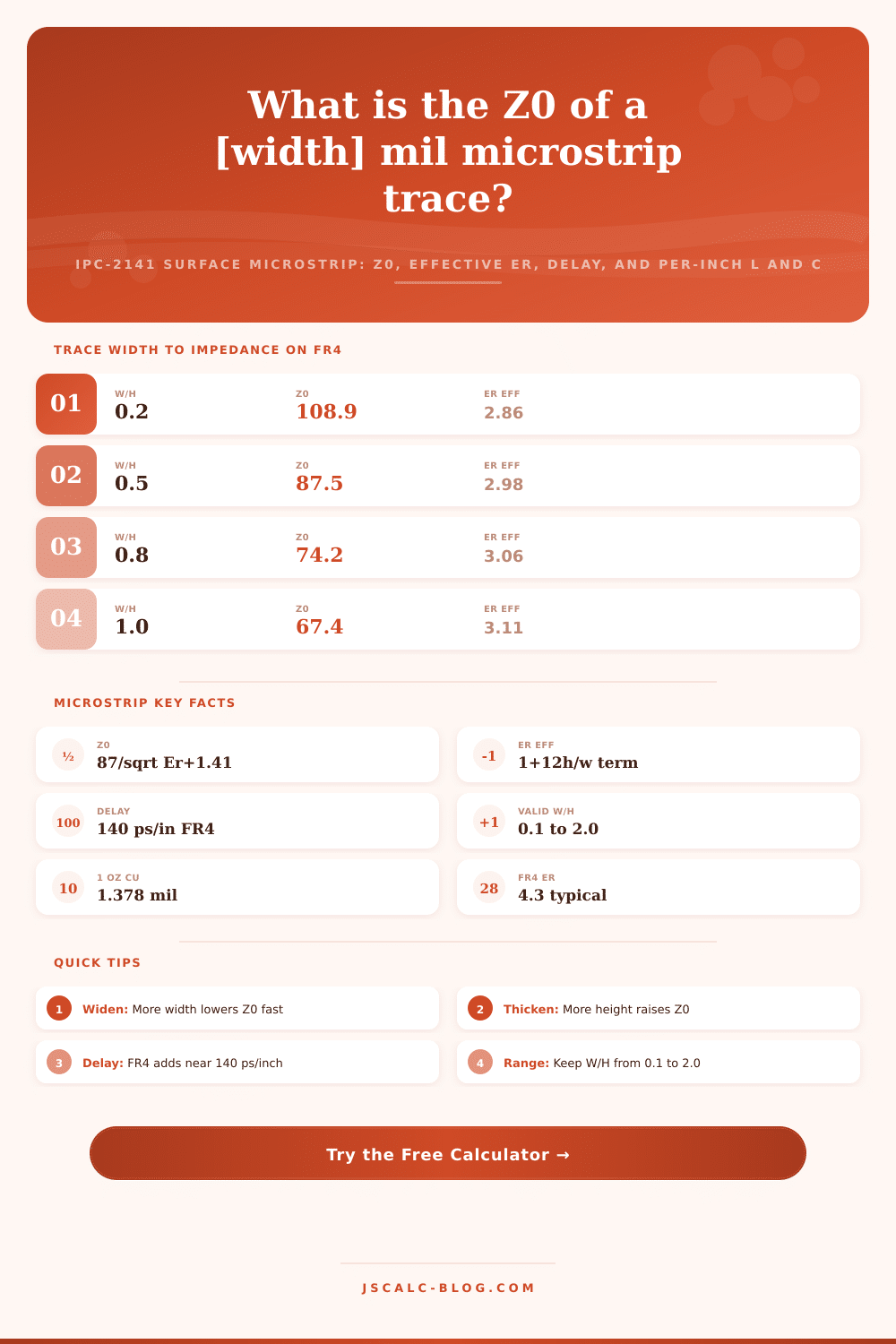
| Trace Width w | Height h | W / H Ratio | Z0 (ohms) | Reads As |
|---|---|---|---|---|
| 2 mil | 10 mil | 0.2 | 108.9 | Very high |
| 5 mil | 10 mil | 0.5 | 87.5 | High Z |
| 8 mil | 10 mil | 0.8 | 74.2 | 75 ohm class |
| 10 mil | 10 mil | 1.0 | 67.4 | Wide 60s |
| 12 mil | 10 mil | 1.2 | 61.6 | 60 ohm |
| 15 mil | 10 mil | 1.5 | 54.5 | Near 50 ohm |
| 18 mil | 10 mil | 1.8 | 48.5 | 50 ohm |
| 20 mil | 10 mil | 2.0 | 44.9 | Edge of range |
🧩Dielectric Constant Reference
| Material | Er (typical) | Er eff at W/H = 1 | Delay ps/inch | Use Case |
|---|---|---|---|---|
| FR4 standard | 4.3 | 3.11 | 140 | General PCB |
| FR4 high Tg | 4.6 | 3.30 | 144 | Lead-free reflow |
| Rogers RO4350B | 3.48 | 2.60 | 127 | RF and microwave |
| Rogers RO4003C | 3.38 | 2.53 | 125 | Low loss RF |
| PTFE Teflon | 2.1 | 1.70 | 105 | Millimeter wave |
| Polyimide flex | 3.5 | 2.61 | 127 | Flex circuits |
| Alumina ceramic | 9.8 | 6.55 | 195 | Hybrid modules |
📏Copper Weight to Thickness
| Copper Weight | Thickness t (mils) | Thickness (microns) | Note |
|---|---|---|---|
| 0.5 oz | 0.689 | 17.5 | Fine HDI lines |
| 1 oz | 1.378 | 35.0 | Most common outer |
| 1.5 oz | 2.067 | 52.5 | Higher current |
| 2 oz | 2.756 | 70.0 | Power planes |
| 3 oz | 4.134 | 105.0 | Heavy copper |
| 4 oz | 5.512 | 140.0 | Bus bars |
📊W/H vs Z0 Comparison Grid (FR4 Er = 4.3, 1 oz)
| W / H Ratio | Z0 (ohms) | Er eff | Delay ps/inch | C (pF/inch) | L (nH/inch) |
|---|---|---|---|---|---|
| 0.2 | 108.9 | 2.86 | 140 | 1.31 | 15.60 |
| 0.4 | 92.4 | 2.94 | 140 | 1.55 | 13.30 |
| 0.6 | 81.6 | 3.01 | 140 | 1.78 | 11.90 |
| 0.8 | 74.2 | 3.06 | 140 | 2.00 | 10.99 |
| 1.0 | 67.4 | 3.11 | 140 | 2.22 | 10.05 |
| 1.2 | 61.6 | 3.15 | 140 | 2.44 | 9.26 |
| 1.5 | 54.5 | 3.20 | 140 | 2.78 | 8.25 |
| 1.8 | 48.5 | 3.25 | 140 | 3.15 | 7.39 |
| 2.0 | 44.9 | 3.27 | 140 | 3.41 | 6.89 |
⚙Formula Breakdown
💡Microstrip Design Tips
When impedance mismatch causes a signal to reflect off a badly matching trace for the first time, it doesn’t look like an error on a schematic; instead, it looks like some strange noise on oscilloscope that you can’t explain. You’ve run your high-speed net in a straight line, and you’ve put components right where the datasheet says, yet data eye’s closed. More likely than not, impedance mismatch is the cause. This means you need to learn that a microstrip trace behave like a transmission line. It depends on its physical geometry (the ratio of copper-to-dielectric below vs. Air above). Here’s how to convert that geometry into four numbers that tell you if your signal lands clean, or all garbled up.
Striplines behave differently than microstrips because they are buried structures rather than being exposed to air. Microstrips is different. They have microstrips exposed to the air on the outside of board. That exposure alters things; it can no longer contain its electric field completely inside the board material. Some part splits off into the air, which has a dielectric constant of approximately 1. The rest moves through the board material, like FR4, whose constant is around 4.3. Instead of seeing the total bulk number of the laminates, the fields see a combination or what’s known as the effective dielectric constant. This combination causes the behavior of microstrip and separates it from other structures like buried striplines. Understanding how to get this blend correct forms core of each calculation since it determines signal velocity as well as characteristic impedance.
How to Calculate Microstrip Impedance
After you enter your substrate properties, copper weight, dielectric height, and trace width, the tool do the math for you using the IPC-2141 standard. This uses an equation that is accurate up to a 2.0 width-to-height ratio. That should of cover about all the practical designs out there. If the trace is narrower than the board thickness, your impedance will spike out of control. Anything wider than that and your model will diverge from reality. The calculator lets you know when you’re outside that sweet spot so you don’t fall prey to trusting something that physics won’t back up. Within its bounds, though, the values returned should be good enough for design review and first pass routing before sending off to manufacturing.
That means your first lever to tune impedance is simply width. Widening a trace predictably reduces its impedance on a typical FR4 board with an eight mil dielectric core. Each additional mil result in about two or three ohms less impedance. That’s a steep trade-off, which makes eyeballing it hard; the tool solves that problem easily. Another factor; albeit a subtler one, is thickness. One ounce of copper is equivalent to 1.378 mils thick, so the calculator translates copper weight to actual thickness. It then factors that thickness into the impedance calculation. Thicker traces retains a bit more charge, which nudges the answer down just a tad. Most designs use one ounce of copper on their outer layers, so that number remains constant unless you change it. For example, you might switch to thin copper for high density interconnects or heavy copper for power distribution.
Another thing worth noting about propagation delay is how it relies on the dielectric constant of the board materials. It’s actualy the effective dielectric constant that matters, which isn’t necessarily the same as the bulk material value. In the case of standard FR4, it comes in around 140 picoseconds/inch. Remember that one; it’ll be handy if you need to make a fast ballpark estimate of how long something will take to get from one place to another. To calculate the total flight time of your signal across all the traces you routed, simply multiply the per-inch delay factor (in our example above) by the distance the signal must fly. Once you understand the rate at which your signals are traveling, you can precisely tune their path lengths instead of fumbling with educated guesses. Length matching your parallel data lines then becomes nothing more than basic math.
The deeper understanding of line interaction with other signals comes from capacitance and inductance per inch. Higher effective dielectric constants increases capacitance. Capacitance can impact edge rate slowing and sensitivity to crosstalk. Lines with lower impedance has more capacitance for each unit length. Higher impedance lines are more inductive. Distributed parameters also shed light on why a via and a stub will load a line and create reflections. They are the parameters used to determine how a surface microstrip behave when under a transient condition. Knowing these parameters lets you predict problems before you see them on production test or on silicon.
For accurate results, the input values must be within the valid range of the model. The IPC-2141 equation applies only if the aspect ratio is between 0.1 and 2.0; too thin, and the trace is narrow enough that fringing fields take over, increasing error; too fat, and the fields distribute differently, needing wider-band models or full-wave simulation software. But, inside the valid window, this calculator provides a full view of one surface line. Choose a preset, tweak the height or width, and read out the breakdown to know which term pushed it. It supplies reliable microstrip numbers in seconds, whether you’re matching lengths on a fast bus or tuning a fifty ohm RF feed. It turns field theory concepts into useful design data.