PCB Trace Impedance Calculator
Choose a controlled-impedance topology, set the target characteristic impedance you need, and this tool solves the trace width that lands it. Uses IPC-2141 microstrip and stripline models to report width, resulting Z0, effective dielectric constant, and propagation delay.
🎯Choose a Solve Mode
📌Real Stackup Presets
📝Geometry and Stackup Inputs
Microstrip references one plane; stripline sits between two planes.
The characteristic impedance you want the trace to hit.
Used only in Width to Z0 mode; solved for you otherwise.
Trace to nearest plane for microstrip; per-side for stripline.
FR4 is roughly 4.2 to 4.5; use your fab stackup value.
Sets copper thickness t = oz × 1.378 mils.
Controls rounding on every result card.
🔢Formula Snapshot
🗂Topology Comparison Grid
| Topology | Typical Er | Z0 Formula | 50 ohm Width | Delay | Use Case |
|---|---|---|---|---|---|
| Surface microstrip | 4.2 to 4.5 | 87/sqrt(Er+1.41) ln(5.98h/(0.8w+t)) | Wider | Faster | Outer RF and antennas |
| Embedded microstrip | 4.0 to 4.4 | Microstrip with higher Er_eff | Medium | Medium | Coated outer layers |
| Symmetric stripline | 4.2 to 4.5 | 60/sqrt(Er) ln(4b/(0.67 pi (0.8w+t))) | Narrower | Slower | Inner critical nets |
| Asymmetric stripline | 4.2 to 4.5 | Offset stripline, dual-plane | Narrower | Slower | Dense inner routing |
| Coated microstrip | 4.1 to 4.5 | Solder mask raises Er_eff slightly | Medium | Medium | Production outer traces |
| Dual stripline | 4.2 to 4.5 | Two offset layers between planes | Narrow | Slower | High layer count boards |
📏Target Impedance to Width on FR4
| Target Z0 | Topology | Height h | Approx Width |
|---|---|---|---|
| 40 ohm | Surface microstrip | 6 mil | 16.5 mil |
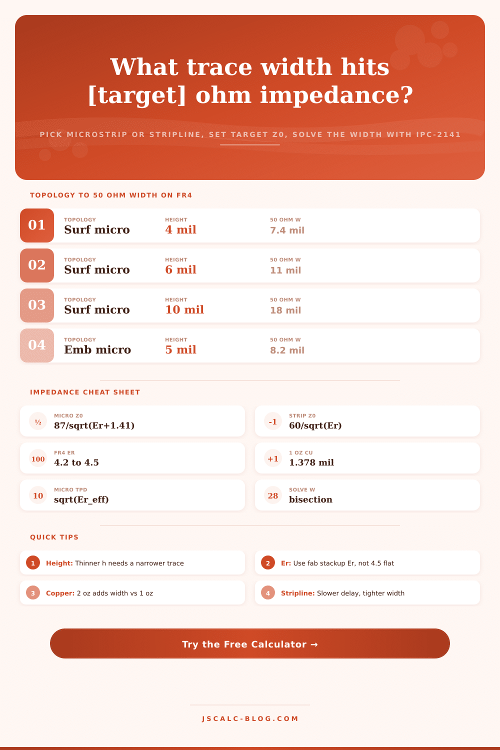
| 50 ohm | Surface microstrip | 4 mil | 7.4 mil |
| 50 ohm | Surface microstrip | 6 mil | 11.0 mil |
| 50 ohm | Symmetric stripline | 10 mil | 6.6 mil |
| 55 ohm | Embedded microstrip | 5 mil | 7.2 mil |
| 75 ohm | Surface microstrip | 10 mil | 10.5 mil |
| 90 ohm | Surface microstrip | 6 mil | 4.0 mil |
| 100 ohm | Symmetric stripline | 12 mil | 3.6 mil |
🧱Dielectric Constant Reference
| Material | Dielectric Er | Loss | Typical Use |
|---|---|---|---|
| Standard FR4 | 4.2 to 4.5 | Moderate | General digital boards |
| High-Tg FR4 | 4.0 to 4.4 | Moderate | Lead-free assembly |
| Rogers RO4350B | 3.48 | Low | RF and microwave |
| Rogers RO4003C | 3.38 | Low | High-frequency analog |
| Isola I-Speed | 3.6 to 3.8 | Low | High-speed digital |
| PTFE Teflon | 2.1 | Very low | mmWave and radar |
📐Copper Weight to Thickness
| Copper Weight | Thickness (mil) | Thickness (um) | Note |
|---|---|---|---|
| 0.5 oz | 0.689 mil | 17.5 um | Fine-pitch inner layers |
| 1 oz | 1.378 mil | 35 um | Most common default |
| 2 oz | 2.756 mil | 70 um | Power and high current |
| 3 oz | 4.134 mil | 105 um | Heavy copper planes |
| 0.25 oz | 0.345 mil | 8.75 um | HDI microvias |
| 4 oz | 5.512 mil | 140 um | Bus bars and busing |
⚙Formula Breakdown by Topology
💡Controlled Impedance Tips
Traditionally, the usual workflow involves guessing a trace width and checking the impedance afterward. With the PCB Trace Impedance Calculator, you select the topology and specify the desired characteristic impedance (50 ohms, 90 ohms, etc.), which means it figure out the trace width for you. That’s more in line with the process used in RF and high-speed designs, where a spec like “I must have 50 ohm traces” provides the number and finding out what that looks like is an exercise in geometry.
Four topologies is paired with a width solver that uses the equations from IPC-2141 to generate one result for use within your layout software. When you get to edge rates where signals are fast enough to act like a transmission line, every copper trace on your printed circuit board becomes a transmission line. If the impedance of that transmission line doesn’t match either the load or the source, it causes timing errors, overshoot, and ringing. This happens because part of the signal reflect back.
How to Find the Right Trace Width for Your PCB
For example, interfaces including Ethernet, PCIe, HDMI, USB and even DDR have controlled impedance specified for them and require the board to maintain that impedance within about 10% tolerance. That means if you don’t hit it, you’re liable to miss by enough that a link that passed on the bench fails in production or under temperature stress. It’s far better to get the trace geometry correct the first time rather then having to re-spin your board once it fails compliance testing.
What sets this tool apart from other single-geometry solvers is the topology dropdown. Microstrip traces are fast, sensitive to variations in their environment and solder mask, and have a single layer of dielectric under them (with air above). Coated or embedded microstrips adds dielectric over the trace and increase the effective dielectric constant while decreasing the impedance. Symmetric striplines sandwiched between two layers of equal insulation make for excellent shielding and repeatability of propagation delay. Asymmetric striplines are off center between the planes and occur frequently on dense boards that don’t have a symmetric stackup. Choosing the proper option will alter both the formula used as well as the width returned by the solver.
Width has that annoying property where it shows up with the copper thickness in a log function. So when you give it a target impedance, it uses something called bisection to calculate the width. This is a solid numerical approach. It starts by bracketing the width with 0.5 mils and 200 mils (a pretty good bracket). Then it checks what the modeled impedance would be at the halfway point and then divides the interval in two and keeps the half that includes the target. After just a couple of dozen iterations, the width is within a small fraction of an ohm of the width that gives you the target impedance. And because it reduces all those field solver concepts to some simple formulas in IPC-2141, this whole thing executes instantly in your browser. If it can’t get close enough in the allowed width range, it says make the dielectric height differrent.
Using the formula, Z0 = 87 / (sqrt(Er + 1.41) * ln(5.98h/(0.8w+t))) The effective dielectric constant is captured in another equation, which describes the way the field splits off into the air above the board. Because the field is completely surrounded on both sides, symmetrical stripline use another coefficient, 60/sqrt(Er). Copper thickness comes straight from the plating weight, since one ounce of copper spreads to about 1.378 mils. Double it with two-ounce copper. That will increase the overall thickness and noticeably increase the width required for equal impedance. You have to choose your copper wisely here and solve first.
The formulas used in this tool are based off IPC-2141 equations. Four result cards is filled with every calculation. The headline answer; the geometry hitting your target; is the required trace width. That’s followed by the impedance card confirming the modeled Z0. This shows how closely the solved width lands on the goal. Next is the effective dielectric constant card, which shows Er_eff. For stripline this will equal bulk Er, but for microstrip it will be lower since some of the field lines travel through air. Finally, the propagation delay card provides both nanoseconds per meter and picoseconds per inch. This gives you all the critical data needed for flight-time budgets and length matching in high-speed digital designs.
One-click loads ten real world stackups into a preset: 50 ohm microstrip on FR4, 90 ohm USB microstrip, and 85 ohm PCIe stripline. A preset configures the topology, target impedance, Er, dielectric height, and copper weight, solving width instantly. It’s a quick look at why the exact same 50 ohm target requires wider traces on thick microstrips than thin buried striplines. From any preset, tweak one input and watch the width it wants shift instanly, building your intuition as to what geometry does to signal integrity.
For normal FR4 shapes, these closed-form models are accurate to a few percent; however, your fab is the last word here. Most fabs only promise controlled impedance within about plus or minus ten percent due to etch tolerance, glass weave effect, and solder mask. Copper roughness also shifts the real impedance. So enter whatever values approximate your actual stackup, using the reference tables for common dielectric constants from low loss Rogers to typical FR4 and for copper weight conversions. Then submit the final stackup to your board house and have them determine production width via their field solver.
Whether they are hobbyists building their first controlled-impedance board, hardware engineers laying out high-speed buses, RF designers matching antenna feeds, or students learning about transmission-line theory, they can go from a target number to a manufacturable trace width in seconds. In one location, it covers asymmetric stripline, symmetric stripline, embedded microstrip, and surface microstrip, so there’s no hunting for another equation on each layer. Pick the topology, enter your target impedance, read the width, check the delay. Guesswork has nothing to do with controlled-impedance design.