PCB Trace Temperature Rise Calculator
Solve the IPC-2221 curve for the temperature rise deltaT of a copper trace at a given current. Enter the current, trace width, copper weight, and layer type to get the conductor rise, the final trace temperature above ambient, the margin to your maximum allowable temperature, and the resistive power dissipated per unit length.
🎯Real Trace Sizing Presets
📝Trace and Current Inputs
Steady DC current the trace must carry.
Finished conductor width. 1 mil = 0.0254 mm.
Sets copper thickness: t = oz x 1.378 mil.
Internal traces run hotter for the same current.
Board temperature around the trace.
Laminate limit, often 105 C for standard FR-4.
Used for total power loss over the run.
Controls rounding on every result card.
🔢Formula Snapshot
📋Copper Weight to Thickness
| Copper Weight | Thickness (mil) | Thickness (mm) | Cross Section 25 mil Wide | Typical Use |
|---|---|---|---|---|
| 0.5 oz | 0.69 mil | 0.0175 mm | 17.2 mil2 | Fine signal RF |
| 1 oz | 1.38 mil | 0.0350 mm | 34.5 mil2 | Standard digital |
| 2 oz | 2.76 mil | 0.0701 mm | 68.9 mil2 | Power and motor |
| 3 oz | 4.13 mil | 0.1050 mm | 103.4 mil2 | High current supply |
| 4 oz | 5.51 mil | 0.1400 mm | 137.8 mil2 | Bus bars and inverters |
| 6 oz | 8.27 mil | 0.2100 mm | 206.7 mil2 | Heavy copper boards |
📈Copper Weight vs Rise, 3A on 25mil External
| Copper Weight | Thickness | Cross Section | Rise deltaT | Final at 25 C |
|---|---|---|---|---|
| 0.5 oz | 0.69 mil | 17.2 mil2 | 110.8 C | 135.8 C |
| 1 oz | 1.38 mil | 34.5 mil2 | 35.4 C | 60.4 C |
| 2 oz | 2.76 mil | 68.9 mil2 | 11.3 C | 36.3 C |
| 3 oz | 4.13 mil | 103.4 mil2 | 5.8 C | 30.8 C |
| 4 oz | 5.51 mil | 137.8 mil2 | 3.6 C | 28.6 C |
| 6 oz | 8.27 mil | 206.7 mil2 | 1.9 C | 26.9 C |
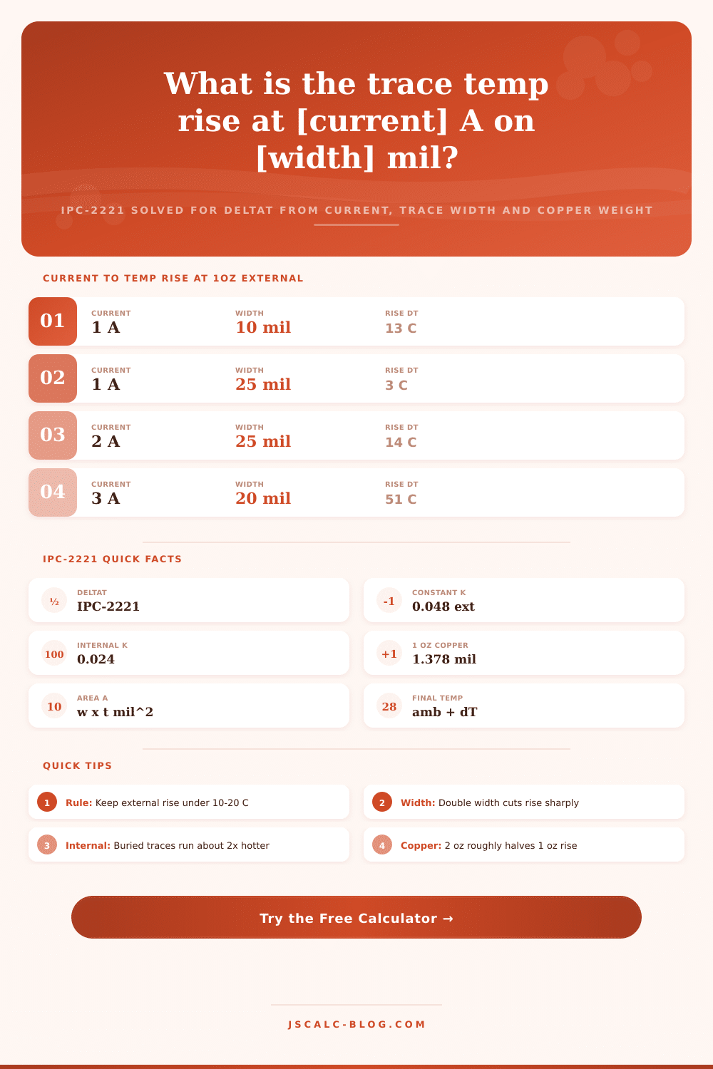
🔥Current vs Temperature Rise, 1oz External Traces
| Current | 10 mil Wide | 25 mil Wide | 50 mil Wide | 100 mil Wide | 200 mil Wide |
|---|---|---|---|---|---|
| 0.5 A | 2.7 C | 0.6 C | 0.2 C | 0.1 C | 0.0 C |
| 1 A | 13.2 C | 2.9 C | 0.9 C | 0.3 C | 0.1 C |
| 2 A | 63.7 C | 14.1 C | 4.5 C | 1.4 C | 0.5 C |
| 3 A | 160.1 C | 35.4 C | 11.3 C | 3.6 C | 1.1 C |
| 5 A | 511.2 C | 112.9 C | 36.0 C | 11.5 C | 3.7 C |
| 7 A | 1098 C | 242.7 C | 77.4 C | 24.7 C | 7.9 C |
| 10 A | 2470 C | 545.8 C | 174.2 C | 55.6 C | 17.7 C |
🌡Recommended Max Temperatures by Laminate
| Material | Tg Glass Transition | Typical Max Conductor | Design Rise Target | Note |
|---|---|---|---|---|
| Standard FR-4 | 130 - 140 C | 105 C | 10 - 20 C | Most common board |
| High Tg FR-4 | 170 - 180 C | 130 C | 10 - 30 C | Lead free assembly |
| Polyimide | 250 C | 200 C | up to 40 C | Aerospace and power |
| Rogers RF | 280 C | 150 C | 10 - 25 C | Microwave laminate |
| Aluminum IMS | 140 C | 120 C | low rise | LED and power modules |
| CEM-1 | 120 C | 90 C | under 10 C | Low cost consumer |
⚙Formula Breakdown (IPC-2221 Solved for deltaT)
💡Trace Thermal Design Tips
Whether it’s a high current digital board, motor driver circuit, or any power supply layout, every hardware engineer who sees a schematic is worried that some thin copper trace will melt when the thing gets put to use. Copper resists electricity, and resistance makes electricity heat up. And if enough of that heat exceeds the tolerance of laminate holding the conductor, the board will fail…often long after you celebrate a successful prototype.
The calculator above do the math for you, using the industry standard IPC-2221 curve and solving directly for temperature rise. Simply input your current, width, type of copper, and layer. It then shows how much power is being dissipated on the trace, your safety margin, and the resulting temperature of the conductor. That goes from a fuzzy guess to a hard number.
How to Stop Your PCB Traces From Overheating
People get this one wrong: Rise isn’t the same thing as final temperature. Final temperature is the degrees a trace is above ambient. That’s your actual goal, right? Say you want something sitting at 55 degrees C. If the board is 25 degrees, then your delta T would be 30 degrees. So how much does it rise? It depends on how big of a cross section of copper there is, how much current you’re pushing through it, and if it’s buried under some dielectric layer or exposed to air. This tool separates out the temperature change. That is what you are really controlling when you choose between width and weight.
What’s underneath? It is an IPC-2221 formula based off measured data that fits the relation: The temperature rise is k (the dissipation efficiency) multiplied by the cross sectional area divided by current. The calculator takes the formula above but re-formats it for you, eliminating the need to loop through yourself. Simply define your load and the geometry, then it gives you the thermal answer.
If the trace sits on the surface being cooled by ambient air then k is zero point zero four eight. If it sits inside the board “buried” in another layer of material, then k plummets to half that number. This simple ratio is why you see buried traces running about double the temperature of an equivalent outer trace. Unless you’re ready to make those inner traces quite a bit wider or move up to heavier gauge copper, keep heavy current out.
Designers also play with the copper weight to weigh it down. An ounce per square foot is about one point four mils. Doubling the weight doubles the thickness, which roughly halves the temperature rise for the same trace width and current. That effectively cuts the temp increase in half at the same size trace and current.
The page has some handy reference tables you can see that make the tradeoff obvious. For example, a twenty five mil trace carrying three amps heats up by more than thirty five degrees with one ounce copper but only by eleven degrees with two ounce. A tiny weight difference and a huge amount of thermal headroom.
To read them, you need to look at each of the four outputs together. The rise gives you the delta; the final temp provides the absolute stress on the material; the power loss indicates the waste of energy as heat; and the margin indicates just how close you are to failure. Generally, most standard FR-4 laminates feature a glass transition temperature of about one-hundred-thirty degrees Celsius, meaning most designers likes to keep the conductor temperatures below one hundred-five degrees for safety.
When your margin goes into the red, you know you’re past that point. Either reduce your load, increase the width of your trace, or distribute the current over multiple parallel traces. A thermal error is an expensive one. It usually shows up after the board is designed and under stress. A marginal trace is free if caught during design but could lead to a costly recall if found in the field.
Start with a preset from the tool, then tweak the parameters for your stackup to see how fast the numbers change. Whether you are working on a rugged power module or a dense digital interface design, knowing exactly what temperature your traces will reach ensures they stay safely below the limit. This gives you peace of mind without the anxiety of not knowing how they will perform thermaly.
Actualy, if you don’t account for this, it could of been a disaster. You should of checked the math more carefuly to avoid any luxurios mistake with the design. If the designer dont watch out, the traces is gone. There is too much heat in the moddern boards and it makes things diffrent than before.