PCB Trace Current Capacity Calculator
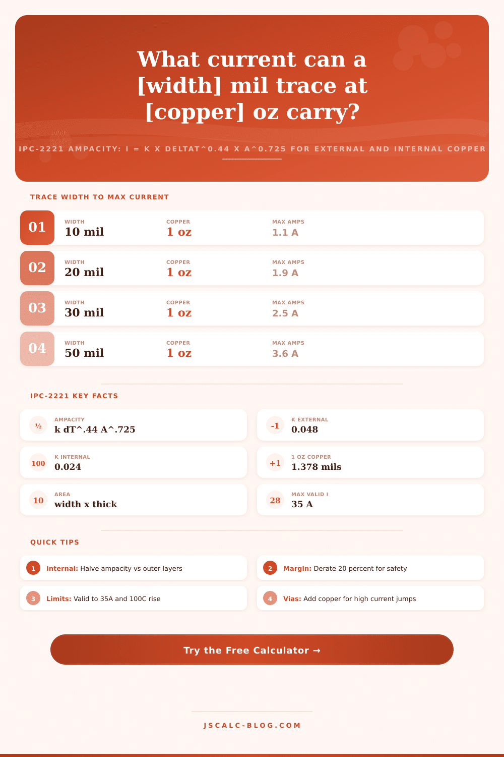
Find the maximum current a copper trace can safely carry using the IPC-2221 ampacity model I = k × deltaT^0.44 × A^0.725. Enter trace width, copper weight, and the temperature rise you allow, and get the max amps, the cross-sectional area, a derated current with your safety margin, plus the trace resistance and voltage drop at full load.
🎯Real Trace Presets
🔧Trace and Thermal Inputs
Conductor width. 1 mil = 0.001 in = 25.4 microns.
Foil weight sets copper thickness = oz × 1.378 mil.
Inner traces run hotter, so k is halved.
Conductor rise above ambient. Common: 10, 20, 30 C.
Board environment. Final trace temp = ambient + rise.
Used for resistance and voltage drop at max current.
Derate the IPC current by this fraction for headroom.
Controls rounding on every result card.
🔢Formula Snapshot
📋External Trace Ampacity at 10°C Rise (1 oz)
| Trace Width | Area (mil²) | Max Current | Typical Use |
|---|---|---|---|
| 5 mil | 6.9 | 0.7 A | Fine signal |
| 8 mil | 11.0 | 0.9 A | Logic routing |
| 10 mil | 13.8 | 1.1 A | General signal |
| 15 mil | 20.7 | 1.5 A | Low power |
| 20 mil | 27.6 | 1.9 A | Small power |
| 30 mil | 41.3 | 2.5 A | Power feed |
| 50 mil | 68.9 | 3.6 A | Power rail |
| 100 mil | 137.8 | 5.9 A | Main bus |
📊Copper Weight to Thickness Reference
| Copper Weight | Thickness (mil) | Thickness (micron) | Area of 20 mil Trace |
|---|---|---|---|
| 0.5 oz | 0.689 | 17.5 | 13.8 mil² |
| 1 oz | 1.378 | 35.0 | 27.6 mil² |
| 1.5 oz | 2.067 | 52.5 | 41.3 mil² |
| 2 oz | 2.756 | 70.0 | 55.1 mil² |
| 3 oz | 4.134 | 105.0 | 82.7 mil² |
| 4 oz | 5.512 | 140.0 | 110.2 mil² |
🗃Width vs Max Current Comparison Grid
| Trace Width | 1 oz @ 10°C | 1 oz @ 20°C | 2 oz @ 10°C | 2 oz @ 20°C | Internal 1 oz @ 10°C |
|---|---|---|---|---|---|
| 8 mil | 0.9 A | 1.3 A | 1.6 A | 2.1 A | 0.5 A |
| 10 mil | 1.1 A | 1.5 A | 1.8 A | 2.5 A | 0.6 A |
| 15 mil | 1.5 A | 2.0 A | 2.5 A | 3.3 A | 0.7 A |
| 20 mil | 1.9 A | 2.5 A | 3.1 A | 4.2 A | 0.9 A |
| 30 mil | 2.5 A | 3.4 A | 4.2 A | 5.6 A | 1.3 A |
| 50 mil | 3.6 A | 4.8 A | 5.9 A | 7.9 A | 1.8 A |
| 80 mil | 5.0 A | 6.7 A | 8.3 A | 11.1 A | 2.5 A |
| 100 mil | 5.9 A | 7.9 A | 9.8 A | 13.1 A | 2.9 A |
| 150 mil | 7.8 A | 10.4 A | 12.9 A | 17.2 A | 3.9 A |
| 200 mil | 9.7 A | 13.0 A | 16.3 A | 21.7 A | 4.8 A |
⚙Formula Breakdown (IPC-2221 Solved for Current)
📏Temperature Rise Multiplier (relative to 10°C)
| Temp Rise deltaT | deltaT^0.44 | Current Factor vs 10°C | Note |
|---|---|---|---|
| 5 °C | 2.04 | 0.74x | Cool, conservative |
| 10 °C | 2.75 | 1.00x | Common baseline |
| 15 °C | 3.28 | 1.19x | Moderate rise |
| 20 °C | 3.72 | 1.35x | Typical power |
| 30 °C | 4.44 | 1.61x | Warm, dense boards |
| 45 °C | 5.30 | 1.93x | Aggressive limit |
💡PCB Current Design Tips
The IPC-2221 standard gives you a way to calculate the maximum amount of current that a given width of copper trace can carry; this helps you avoid burn marks on your prototype and prevents your design from slowly thermally degrading over years in service. All you have to do is know the width of the trace and its copper weight, and then enter a desired temperature increase to find the ampacity. The tool provides industry standard relationship plus throws in some voltage drop and resistance information as well. So now you get entire thermal/electrical picture all in one place.
The formula assume a curve fit based off the cross sectional area and the temperature rise due to current. The more copper surface area exposed to free air, the better it dissipates heat. K = 0.048 if the trace is on the outside of the board and in an external layer. If it’s inside the board sandwiched between layers of dielectric, there’s no direct path from the copper to free air. This causes k to decrease to 0.024 which reduces current capability by about half. This is a brutal fact of life for tightly-packed multi-layer board.
How to Use the IPC-2221 Calculator
For example, the calculator use your entries to compute area first and then runs formula. Weight per square foot of copper on a board is entered as ounces per square foot, and each ounce becomes a layer 1.378 mils thick. Half ounce copper is 0.689 mils, one ounce is 1.378 mils, and two ounces is 2.756 mils. Multiply the copper thickness by the trace width, and that’s the cross-sectional area. A trace that is 20 mils wide using one-ounce copper has a cross-sectional area of 27.6 square mils. This number go straight into the ampacity equation. You’ll see it right there on the tool’s result card so you can’t get lost in the geometry.
Let’s say we’re routing a 20 mil external trace in one ounce copper, and we don’t mind a 10 degree Celsius increase. We come up with about 1.9 amps. If we bump the increase up to 20 degrees then it increases to about 2.5 amps.
Why does this matter? It matters because the amount of current you can carry depends on your trace’s geometry and thickness. That’s why both the amount of copper and the allowed temperature rise are important. Allowing more heat lets you use a higher current for the same geometry, but do you want to risk that extra heat on your sensitive components?
There is four cards per calculation. One figures out the maximum IPC current at your specific conditions of temperature rise, layer, copper weight, and width. Another card display the cross sectional area in case you want to double check that the geometry looks right. The third card applies your safety margin and tells you what the recommended derated current would be. That’s key: the raw formula predicts a steady-state condition, but you need a safety margin to account for things like warmer ambient air, heat-trapping solder mask, and aging copper. Finally, the fourth card combine resistance and voltage drop, using copper resistivity to compute how many millivolts the trace loses at its maximum current. It also has a detailed breakdown panel showing all the numbers it plugged into formulas; making this tool not only a calculator but also a back-of-the-napkin check.
Why is there a safety margin? Because in the real world your board will have warm ambient air, aged copper, nearby components, and solder mask to trap heat. Running it at 1.5-1.6 amps continuously (half way) gives some extra headroom for the unexpected. The calculator explicitly displays this as a safety margin field. Plug in 20% and your recommended current card will display 80% of raw number. That’s conservative enough to keep you sane, but not so much that you need to recalculate whenever you adjust any parameters.
The other extremely frequent error is using an inner-layer trace as though it’s an outer layer. Because inner-layer traces are sandwiched inside dielectric material, you get more heat per amp for a given trace size. That’s easy to see from the comparison grid: that same 20 mil trace can handle around 0.9 amps with 10 degrees rise on an inner layer vs. It can handle around 1.9 amps on an outer layer. Widen your inner traces significantly if this is where your power distribution lives (or better yet, go multiple parallel paths, pour out some copper, etc.)
Ampacity is only half the story. You can get away with pushing a lot of current through a long, narrow trace … but it’s wasting all that power while also dropping the voltage your load receives. Here, the calculator calculates resistance based on cross section and length, then multiplies by max current to determine the drop. Even one hundred milli-volts of drop may be significant if you’re running a sensitive rail. Having both drop and resistance displayed alongside ampacity lets you judge whether an otherwise-thermally-perfect trace is electrically workable.
This chart set was developed for the IPC-2221 standard, bounded roughly at 100 degree C rise and 35 amps. Outside these limits, board construction is most important factor. Use thermal simulation and latest standard. Inside the limits of the chart, it’s a solid first pass.
You have your design. Enter the settings for width, copper, and allowed rise. In seconds, the calculator returns voltage drop, the safe working maximum current, and a pretty good max current. That is the answer all designers ask for, providing a clear engineering decision instead of guesswork.