Differential Pair Impedance Calculator
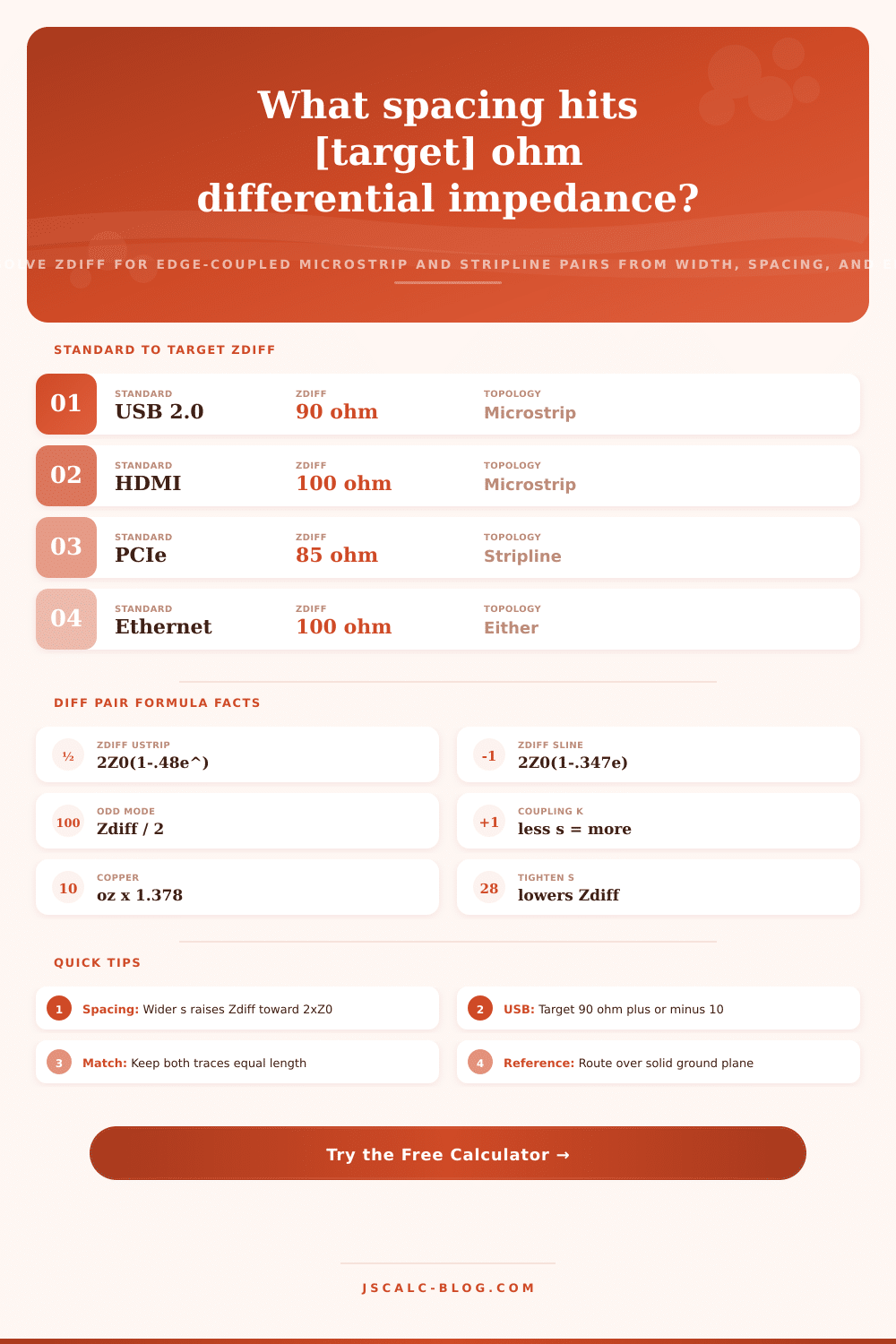
Compute differential impedance Zdiff for edge-coupled microstrip and stripline pairs from trace width, edge-to-edge spacing, dielectric height, copper weight, and Er. Get single-ended Z0, odd-mode impedance, the coupling term, and the spacing needed to hit a target like USB 90 ohm or HDMI 100 ohm.
🔗Choose a Topology
🎯Real Interface Presets
📝Pair Geometry Inputs
Width of each single trace in the pair, in mils.
Gap between the inner edges of the two traces.
Microstrip: trace to reference plane. Stripline: use plane spacing b.
Sets copper thickness t = oz x 1.378 mils.
FR-4 is about 4.2 to 4.5; Rogers laminates run lower.
Standard target, such as 90 for USB or 100 for HDMI.
Controls rounding on every result card.
🔢Formula Snapshot
📋Standard Interface Target Impedances
| Interface | Target Zdiff | Odd Mode | Typical Topology |
|---|---|---|---|
| USB 2.0 | 90 ohm | 45 ohm | Microstrip |
| HDMI / DVI TMDS | 100 ohm | 50 ohm | Microstrip |
| PCI Express | 85 ohm | 42.5 ohm | Stripline |
| Gigabit Ethernet | 100 ohm | 50 ohm | Either |
| LVDS | 100 ohm | 50 ohm | Either |
| DDR4 differential | 80 ohm | 40 ohm | Stripline |
| SATA | 100 ohm | 50 ohm | Microstrip |
| DisplayPort | 100 ohm | 50 ohm | Stripline |
📊Spacing Effect on Coupling and Zdiff
| Ratio s / h | Coupling Term | Coupling | Zdiff vs 2xZ0 | Meaning |
|---|---|---|---|---|
| 0.25 | 0.48 e^-0.24 | Strong | 62 percent | Very tight pair |
| 0.50 | 0.48 e^-0.48 | Strong | 70 percent | Tight coupling |
| 1.00 | 0.48 e^-0.96 | Moderate | 82 percent | Common spacing |
| 1.50 | 0.48 e^-1.44 | Light | 89 percent | Loose pair |
| 2.00 | 0.48 e^-1.92 | Light | 93 percent | Weak coupling |
| 3.00 | 0.48 e^-2.88 | Minimal | 97 percent | Nearly isolated |
| 4.00 | 0.48 e^-3.84 | Minimal | 99 percent | Almost no coupling |
🗄Standard vs Target Zdiff Comparison Grid
| Standard | Target Zdiff | Odd Mode | Single-Ended | Topology | Tolerance |
|---|---|---|---|---|---|
| USB 2.0 | 90 ohm | 45 ohm | ~50 ohm | Microstrip | plus/minus 10% |
| HDMI TMDS | 100 ohm | 50 ohm | ~55 ohm | Microstrip | plus/minus 10% |
| PCIe Gen3 | 85 ohm | 42.5 ohm | ~48 ohm | Stripline | plus/minus 10% |
| Ethernet | 100 ohm | 50 ohm | ~55 ohm | Either | plus/minus 10% |
| LVDS | 100 ohm | 50 ohm | ~55 ohm | Either | plus/minus 10% |
| DDR4 | 80 ohm | 40 ohm | ~45 ohm | Stripline | plus/minus 10% |
| SATA | 100 ohm | 50 ohm | ~55 ohm | Microstrip | plus/minus 10% |
| DisplayPort | 100 ohm | 50 ohm | ~55 ohm | Stripline | plus/minus 10% |
| MIPI D-PHY | 100 ohm | 50 ohm | ~55 ohm | Microstrip | plus/minus 10% |
| CAN FD | 90 ohm | 45 ohm | ~50 ohm | Microstrip | plus/minus 10% |
⚙Formula Breakdown
💡Differential Routing Tips
When everything is designed at high speeds, every detail counts. A small change in signal trace impedance can transform a pristine signal into an unusable noisy mess that never settles down. To prevent this from happening, designers uses a kind of safety net called differential signalling.
Instead of sending one voltage along a trace, they sends two equal but opposite voltages along adjacent traces. By subtracting one line from the other, the receiver filters out common noise while accepting only difference between them. While this system tolerates ground shift and rejects interference, it also requires precise measurements. The pair should show precisely differential impedance defined in the standard (typically 90 or 100 ohms).
How Differential Impedance Works
Understanding how to make that happen isn’t a matter of gut instinct; it’s about controlling electromagnetic coupling. That’s what this calculator does for you. Differential impedance (Zdiff) isn’t double the impedance of a single trace; that’s why specialized calculators are required to calculate it! When you route a differential pair, there is magnetic and electrical interaction between two traces. Because they’re close to each other, their field lines start to couple more strongly as they near one another.
In fact, when they couple closely enough, the differential impedance becomes less than expected 2x Z0. That’s because it couples. And that’s why you want to route differentially! This is why differential impedance is such an important concept. Understanding it helps because a slight shift in trace spacing can destroy signal integrity.
Odd mode impedance is exactly half Zdiff. The calculator accounts for all those complicated interactions, and you don’t need to struggle with exponential decay terms. Typically most designers use some form of stripline or edge coupled microstrip structure. With microstrip the pair is located above a reference plane on an outer layer. Half of field is exposed to air and half to the dielectric.
With stripline it’s buried between two ground planes offering improved shielding but needing more inner layers. Each of these options impacts all variables in the equation. For example, if you’re using microstrip, then you’d be concerned about height from the trace to the closest plane. If you use stripline, then your concern would be distance between the top and bottom reference planes.
Depending upon what you choose, the tool will switch which internal formula it uses. The tool switches its internal formulas based on your selection, adjusting for how electric fields distribute through the laminate. That makes a difference when trying to achieve a tight tolerance window on a dense board.
The strongest lever in differential design is spacing. As you increase trace spacing, coupling decreases. So, Zdiff approaches double it’s single-ended value. On the other hand, decreasing spacing increases coupling, pulling Zdiff downward. Because this effect is so sensitive, even small variations in manufacturing tolerances can exceed spec limits.
For example, a slight variation in etching or lamination thickness can shift your impedance enough to violate spec limits. The calculator enables iteration to determine optimal spacing for your desired impedance. You provide the fixed stackup and width. The calculator solves the reverse of the usual guess-and-check problem. It tells you exactly how far apart to space your traces instead of making you guess what your resulting impedance will be.
In reality, interfaces have non-negotiable targets. For example, USB 2.0 specifies 90 ohms; HDMI, Ethernet, and LVDS generally expect 100 ohms; PCIe is often 85 ohms to balance density and speed. Each of these standards assumes a certain level of coupling and reflection control. When they get 110 instead of 100 ohms on their board, they’ll observe reflections. Those reflections damage the eyes in the data stream and raise bit error rates.
The tool’s built-in presets include realistic starting shapes for many common interfaces. This way you have a baseline that takes into consideration typical values for copper weight, as well as dielectric constant for FR-4. From there, you can tweak away. Adjust for different materials, such as Rogers laminates. Adjust for heavier copper.
Another key thing to consider here is the length match. Length matching is also directly related to impedance control. If the impedance is perfectly matched but the lengths don’t match, then there will be skew between the two traces which turns differential signals into common-mode noise. So keep the trace lengths within a few mils of each other to maintain signal integrity and length match.
And route these traces symmetrically across a continuous, solid ground plane. Do not split the reference layer underneath the trace pair. This causes the return current to take longer paths and adds inductance. These layout practices matter as much or more than the actual impedance numbers do. Impedance control is all about understanding the physics of the fields surrounding your copper. Respect it, and things will go well; fail to do so and the headaches will stay.
You could of made this happen by doing the following:
• Start with the correct spacing.
• Match up your length differences. Keep your ground plane consistent.
The tool provides a quick pass at the numbers you can trust, saving hours of hand calculations by using closed-form equations that approximate transmission line reality to within 5 to 10 percent. An excellent start, but always confirm against your fabricator’s stackup calculator or a field solver prior to final release.