Solder Paste Volume Calculator
Size your SMT stencil print with real numbers: get the deposit volume per aperture from aperture area times stencil thickness, scale it to total paste volume across every pad, convert to paste mass in grams using paste density, and check the IPC-7525 area ratio to see whether each aperture will release cleanly.
🎯Real Stencil Printing Presets
🔧Aperture & Paste Inputs
Match the stencil opening for the footprint you print.
Long dimension of a rectangular opening.
Short dimension of a rectangular opening.
Edge length for a square aperture.
Opening diameter for a round BGA or via pad.
Foil thickness; also the deposit height.
1 mil = 25.4 um. Common foils are 100 to 150 um.
How many identical openings the print covers.
No-clean SAC305 paste is near 4.4 to 4.7 g/cm3.
Fraction of aperture volume actually deposited.
Solder by volume; Type 3/4 paste is about 0.50.
🔢Formula Snapshot
📋Area Ratio by Square Aperture
| Square Side | Stencil 100 um | Stencil 120 um | Stencil 150 um |
|---|---|---|---|
| 0.20 mm | 0.50 fail | 0.42 fail | 0.33 fail |
| 0.25 mm | 0.63 fail | 0.52 fail | 0.42 fail |
| 0.30 mm | 0.75 pass | 0.63 fail | 0.50 fail |
| 0.35 mm | 0.88 pass | 0.73 pass | 0.58 fail |
| 0.40 mm | 1.00 pass | 0.83 pass | 0.67 pass |
| 0.50 mm | 1.25 pass | 1.04 pass | 0.83 pass |
| 0.60 mm | 1.50 pass | 1.25 pass | 1.00 pass |
◯Area Ratio by Round Aperture
| Diameter | Stencil 100 um | Stencil 125 um | Stencil 150 um |
|---|---|---|---|
| 0.20 mm | 0.50 fail | 0.40 fail | 0.33 fail |
| 0.25 mm | 0.63 fail | 0.50 fail | 0.42 fail |
| 0.30 mm | 0.75 pass | 0.60 fail | 0.50 fail |
| 0.35 mm | 0.88 pass | 0.70 pass | 0.58 fail |
| 0.40 mm | 1.00 pass | 0.80 pass | 0.67 pass |
| 0.45 mm | 1.13 pass | 0.90 pass | 0.75 pass |
| 0.50 mm | 1.25 pass | 1.00 pass | 0.83 pass |
📏Stencil Thickness Reference
| Thickness (um) | In Mils | Typical Use | Finest Pitch |
|---|---|---|---|
| 75 um | 3.0 mil | Ultra fine 0201 / 0.3 CSP | 0.30 mm |
| 100 um | 3.9 mil | 0402 and 0.4 mm BGA | 0.40 mm |
| 120 um | 4.7 mil | General SMT mixed board | 0.50 mm |
| 127 um | 5.0 mil | Standard 0.5 mm QFP | 0.50 mm |
| 150 um | 5.9 mil | Larger passives, connectors | 0.65 mm |
| 200 um | 7.9 mil | Power pads, thermal tabs | 0.80 mm |
🗃Aperture to Deposit Comparison Grid
| Component | Aperture | Stencil | Aperture Vol | Deposit Vol | Paste Mass | Area Ratio |
|---|---|---|---|---|---|---|
| 0201 chip | 0.30 x 0.30 | 100 um | 0.0090 mm3 | 0.0041 mm3 | 0.041 mg | 0.75 pass |
| 0402 chip | 0.50 x 0.60 | 120 um | 0.0360 mm3 | 0.0166 mm3 | 0.166 mg | 0.68 pass |
| 0603 chip | 0.80 x 0.90 | 127 um | 0.0914 mm3 | 0.0421 mm3 | 0.421 mg | 1.11 pass |
| 0.4 BGA | 0.25 dia | 100 um | 0.0049 mm3 | 0.0023 mm3 | 0.023 mg | 0.63 fail |
| 0.5 BGA | 0.30 dia | 120 um | 0.0085 mm3 | 0.0039 mm3 | 0.039 mg | 0.63 fail |
| 0.5 QFP | 0.28 x 1.40 | 127 um | 0.0498 mm3 | 0.0229 mm3 | 0.229 mg | 0.55 fail |
| QFN pad | 0.25 x 0.60 | 100 um | 0.0150 mm3 | 0.0069 mm3 | 0.069 mg | 0.35 fail |
| 1206 LED | 1.00 x 1.10 | 150 um | 0.1650 mm3 | 0.0759 mm3 | 0.759 mg | 1.31 pass |
| 0.8 conn | 0.45 x 1.60 | 150 um | 0.1080 mm3 | 0.0497 mm3 | 0.497 mg | 0.59 fail |
| Thermal tab | 2.00 x 2.00 | 150 um | 0.6000 mm3 | 0.2760 mm3 | 2.760 mg | 3.33 pass |
⚙Formula Breakdown
💡Stencil Printing Tips
A solder paste volume calculator takes a stencil’s aperture geometry to generate four values. These include the volume of paste deposited into each opening, total amount of paste across the board, weight in grams, and IPC-7525 area ratio. These values predict whether an aperture will release its deposit cleanly or not. Simply input the paste density, foil thickness, and aperture size and shape. Results are reported in your printer/reflow oven’s preferred units which helps you try to prevent bridges on fine-pitch components or skips on tiny 0201 chips.
A stencil is a very thin piece of metal foil with holes punched out so that solder paste can be forced through it. For each hole, the solder paste forms a brick shaped like the aperture. The aperture is a right angle prism. So, amount of solder paste laid down is the area of the aperture times the thickness of the foil. Every calculation involving paste depend on that relationship. A 0.5 x 0.6 mm rectangular aperture in 0.12 mm foil has a volume of 0.036 cubic millimeters. Multiply by the number of same-sized apertures to get overall volume. That’s the amount used up and tells you how frequently you need to refill your squeegee. It also help you calculate how much paste is needed for a production batch. This prevents you from wasting solder paste or having too little.
How to Use a Solder Paste Volume Calculator
Three typical stencil shapes are supported in the calculator. Capacitor and resistor pads is rectangular. To find their area, you multiply width times length. QFN and BGA land patterns are squares. Find their area by squaring the side. Ball grid array balls are typically round. Area is pi over four times the diameter squared.
Why does this matter? Each different shape affects both the volume and the area ratio printed. For example, a round 0.3 mm aperture prints differently than a square of the same size. When you change the shape, the tool automaticly picks up that difference and saves you from having to get the geometry wrong manually.
So how do you know if your paste is going to come out of the aperture? You don’t base that on volume. You base that on area. And that’s called the area ratio. That’s the critical quality measure for prints on PCBs. Why? It looks at both the area inside the opening and the area outside the opening. Adhesion differs between the opening area, where the paste sticks to the pad, and the wall area which sticks to the foil.
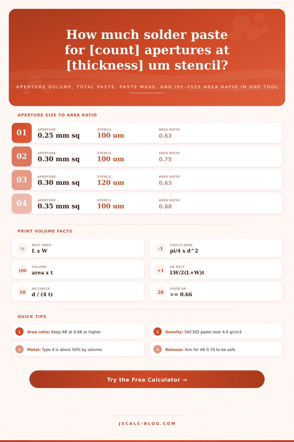
For a rectangular hole it’s calculated as length x width/ (2*length+width)*thickness. For a round hole, it’s easier: diameter/(4*thickness). If the ratio is high the paste cleanly releases into the pad. If it’s low then it will stick or smear in the opening. By convention, a bare minimum aperture area ratio (AAR) should of be 0.66. For good release with most electropolish stencils, we like an area ratio of 0.70+. Our calculator tests for these values. A ratio of 0.70 or higher means it’s a clean pass. Between 0.66 and 0.70 it says “warn”; that’s marginal but might work. A ratio below 0.66 is a fail. This information is useful during the design stage rather than after a print failure occurs. So if you get 0.63 for a 0.3 mm square on 0.12 mm foil, you’ll know to go thinner. Going down to 0.10 mm foil gets you a 0.75 for that same aperture.
Instead of cubic millimeters, cubic centimeters are commonly used in purchasing and process control. Paste density is needed for the conversion from volume to mass. For example, common no-clean SAC305 lead-free paste is roughly 4.6 grams/cc. A cubic millimeter is one-thousandth of a cubic centimeter. Therefore, 0.036 cubic millimeters of paste weighs about 0.166 milligrams. Across thousands of apertures on an entire panel, those milligrams accumulate. With this knowledge, you can accurately budget paste.
Theoretical volume isn’t what gets deposited. Some amount less than 100 percent will get transferred to real prints. A good design typically transfers 80-95 percent. We apply your selected transfer efficiency in the calculator. This also applies to the typical metal volume fraction, which is roughly 0.50 for most Type 3 and Type 4 pastes and represents the leftover solid solder volume once the flux burns out during reflow. That’s what determines fillet size and joint standoff height. Knowing how much wet paste is printed next to that post-reflow number lets you fine-tune the aperture design. You want correct joint, not simply the printed paste.
To speed up use in practice, it includes presets for common footprints they regulary deal with: 0402 and 0201 chips. It also includes presets for common parts like QFN center pads and 0.4 and 0.5 mm pitch BGAs. Each one presets a realistic count of openings, foil thickness, and opening size. You can load up a new fine-pitch design and get quick check of it. Or maybe you’re having some line skips and want to diagnose? Seconds later, the calculator gives you geometry-backed numbers. It turns those vague dimensions into real process information. This ensures your boards come out of the printer with just enough paste for good joints. You must also avoid using too much which will cause defects. That’s the tricky part of achieving reliable SMT assembly.