PCB Panel Utilization Calculator
Estimate how many circuit boards fit on a fabrication panel using true 2D bin-packing. Enter your panel size, board size, edge rail margin, and inter-board gap, then get boards per panel, panel area utilization, wasted copper-clad material, and the number of panels needed to fill an order, with optional 90 degree rotation for the best yield.
📌Real Panel & Board Presets
📏Panel & Board Inputs
All sizes below use this unit; areas convert automatically.
Full copper-clad panel width, e.g. 457 mm (18 in).
Full panel height, e.g. 610 mm (24 in).
Finished width of one individual PCB.
Finished height of one individual PCB.
Tooling/handling border removed from each of the 4 sides.
Spacing between adjacent boards for scoring or routing.
Rotating boards can raise yield when sizes are uneven.
How many finished boards the order requires.
🔢Method Snapshot
⚙How the Math Works
📋Standard Fabrication Panel Sizes
| Panel Name | Imperial | Metric (mm) | Gross Area |
|---|---|---|---|
| Small proto | 9 x 12 in | 229 x 305 | 0.070 m2 |
| Half panel | 12 x 18 in | 305 x 457 | 0.139 m2 |
| Standard full | 18 x 24 in | 457 x 610 | 0.279 m2 |
| Large full | 21 x 24 in | 533 x 610 | 0.325 m2 |
| Extended | 18 x 48 in | 457 x 1219 | 0.557 m2 |
| Metric working | ~15.7 x 20.9 | 400 x 530 | 0.212 m2 |
| Metric large | ~20.5 x 24.4 | 520 x 620 | 0.322 m2 |
📈Edge Rail & Gap Guidance
| Assembly Type | Edge Rail | Board Gap | Best Method | Notes |
|---|---|---|---|---|
| Hand solder / proto | 0-5 mm | 2-3 mm | V-score | Minimal handling needs |
| Reflow, conveyor SMT | 5-10 mm | 2 mm | V-score | Rails carry the array |
| Wave / selective | 8-12 mm | 3 mm | Tab-route | Room for fingers/pallet |
| Irregular outline | 10 mm | 2-3 mm | Tab-route | Mouse-bites on tabs |
| Fiducials + tooling | 10 mm | 2 mm | V-score | 3 fiducials, 2 tooling holes |
| Flex / rigid-flex | 10-15 mm | 3-5 mm | Laser rout | Stress relief spacing |
🗃Boards Per Panel Comparison Grid
| Board Size | Panel (mm) | Rail | Gap | Boards | Utilization |
|---|---|---|---|---|---|
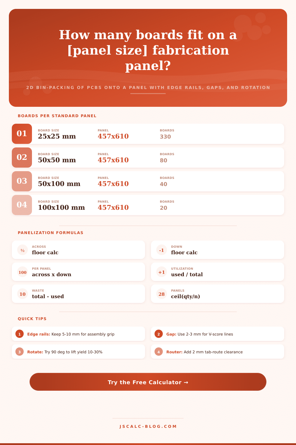
| 25 x 25 mm | 457 x 610 | 10 mm | 2 mm | 330 | 74.0% |
| 30 x 30 mm | 457 x 610 | 10 mm | 2 mm | 224 | 72.3% |
| 40 x 60 mm | 457 x 610 | 10 mm | 2 mm | 96 | 82.6% |
| 50 x 50 mm | 457 x 610 | 10 mm | 2 mm | 80 | 71.7% |
| 50 x 100 mm | 457 x 610 | 10 mm | 2 mm | 40 | 71.7% |
| 60 x 80 mm | 457 x 610 | 10 mm | 2 mm | 48 | 82.6% |
| 75 x 100 mm | 457 x 610 | 10 mm | 2 mm | 24 | 64.6% |
| 100 x 100 mm | 457 x 610 | 10 mm | 2 mm | 20 | 71.7% |
| 100 x 160 mm | 457 x 610 | 10 mm | 2 mm | 12 | 68.8% |
| 18 x 18 mm | 457 x 610 | 10 mm | 2 mm | 625 | 72.6% |
📐Unit & Area Conversions
| Quantity | Equals | In Base Unit | Note |
|---|---|---|---|
| 1 in | 25.4 mm | 25.4 mm | Length |
| 1 mm | 0.03937 in | 0.03937 in | Length |
| 1 in2 | 645.16 mm2 | 645.16 mm2 | Area |
| 1 mm2 | 0.00155 in2 | 0.00155 in2 | Area |
| 1 m2 | 1,000,000 mm2 | 1550 in2 | Area |
| 1 ft2 | 144 in2 | 92903 mm2 | Area |
💡Panel Yield Tips
Rarely does a printed circuit board travel solo. More often than not, it’s part of a family that travels together on a big sheet of identical copies known as the fabrication panel.
How many do you put on there? That’s the unit cost. Half empty or full, you paid for all of it. This calculator view the layout as a two-dimensional packing problem. It will return four key numbers. These are the total panels needed for your order, wasted material, panel utilization, and boards per panel.
How to Save Money on PCB Panels
Cost depends on panel usage. Fabricators is paid per sheet (panel) rather than per unit. Etching, plating, and imaging is all done at a flat rate for an 18 by 24 inch panel. Divide that total by however many board they can fit onto it. Eighty? Good deal. Seventy two? Each board take up more of the total cost. This makes a huge difference over tens of thousands of units.
That’s why buyers always want to fill each row and column, and the calculator does the math for you, no guessing about what space works and doesn’t. First, it takes out wasted area by reducing dimensions to exclude reflow sacrificial strips called “edge rails.” The useable width is the panel width minus twice the rail depth. Next it divides that into a rectangle and fills that with a grid of boards, allowing a little bit of space for routing/scoring in-between.
Boards-across = Floor of useable-space/(Board-size+Gap)
So it’s just a matter of dividing some geometry. But what it demonstrates is exactly how many square inches of copper you’re throwing away compared to buying. The result can be very different with rotation. Boards of one shape are packed differently depending on how they’re rotated. A tall skinny board may fit into seven columns in landscape and ten in portrait.
If you enable rotation, the tool calculates both ways. Then it retains the better option (i.e. It retains the option that packs the most boards. Just this one toggle frequently adds another 10-30 percent. There’s no downside to checking; just leave rotation turned-on unless the placement of connectors dictates a fixed heading.
Here’s what you read on it:
First card = Array size in inches and boards/panel,
Second card = Panel Utilization (percentage of live board vs. Gross panel area)
Third card shows Wasted Area, which includes gaps, rails, and trimmed offcuts.
Fourth card shows Panels Needed. To find this, divide your order quantity by the yield and round up. A partial last panel is still considered a full sheet.
Much of that output comes down to two inputs: inter-board gaps and edge rails. For edge rails, five to ten millimeters on each side is typical. Ten millimeters allows space for tooling holes and fiducial marks; five should be enough for an automated surface-mount line to grab onto. The board gap depends on the separation method. If you’re tab-routed, you’ll need some clearance (about two to three millimeters) along with mouse-bite tabs to secure irregular outlines. V-scored boards requires a narrower channel (two to three millimeters), as the blade scores a shallow groove from both directions.
Reducing your edge rails from ten to five millimeters creates about twenty additional millimeters in each direction. This extra space is sometimes enough to fit another full row of small boards. Let’s look at typical panels which have ten millimeter rails and are 50 by 50 millimeter IoT modules with a two millimeter gap between them. So usable width is 50 minus 2 times 9, or 437 millimeters. Down is what? The floor of 439 divided by 52 is eight boards across. There are eleven rows down for useable height. There are eighty-eight boards per panel. You need fifty-seven panels for an order of five thousand boards.
And if you would of missed your chance to rotate or lock in another board shape, that could be sixty-five panels. Sixty-five minus fifty-seven is just plain waste. The calculator also does all of this conversion for you, using whatever unit you like (millimeters and inches are both accepted on the fabricator’s data sheet). A square inch equals 645.16 square millimeters; 1 inch = 25.4 millimeters. Type in your size in either inches or centimeters and it will switch them over for you into the other unit when calculating area. So, for example, put in 2-inch boards for an 18 by 24 inch panel, or vice versa; the same goes for metric equivalents. The results will be reported in whichever unit you choose.
Reference tables group together popular panel sizes and rail tips. With those, you can reference knowns and test any given layout before passing a design off to manufacturing. Choose a starting Preset similar to your application. Scale the board size, rails, gap, or order qty to match the actual design. Observe how the Panels Needed/Boards Per Panel updates. As you change each parameter, the output tells you instantly if it’s better to rotate the board a millimeter or cut the rails shorter.
It’s not a complete CAM step-and-repeat solution but more of a quick utility to help plan. Check the resulting layout in your fabricator’s design rule checker before cutting just to be sure about scoring direction and minimum tab spacing. If used properly, it estimates your panel utilization as a number that you can confidentally tweak to maximize yield and get every square millimeter of copper paying its due.