PCB Layer Stackup Thickness Calculator
Add up every layer in your board stackup to find total finished thickness. Enter the number of copper layers and copper weight, the count and thickness of your cores and prepreg sheets, and the soldermask per side. The tool returns total board thickness in mm and mil, the copper contribution, and the through-hole via aspect ratio so you can check it against fab limits before you order.
🎯Real Stackup Presets
📝Stackup Inputs
Count every copper plane. A 4-layer board has 4 copper layers.
1 oz = 34.79 um of finished copper per layer.
Glass-epoxy cores clad with copper on both faces.
Typical FR-4 core runs 0.1 to 1.0 mm; heavy cores go higher.
Resin-glass bonding sheets between cores and foils.
1080 ~ 0.075, 2116 ~ 0.105, 7628 ~ 0.185 mm.
Applied to both outer faces, ~0.015 to 0.025 mm each.
Smallest plated drill; sets the via aspect ratio.
Controls rounding on the mm and mil result cards.
🔢Key Constants
📋Copper Weight to Thickness
| Copper Weight | Per Layer (um) | Per Layer (mil) | Common Use |
|---|---|---|---|
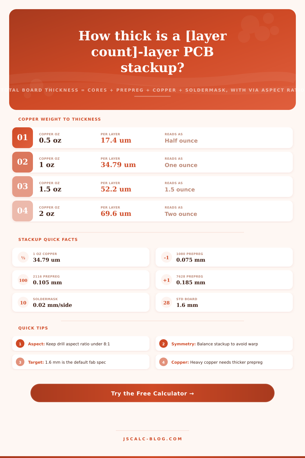
| 0.5 oz | 17.4 um | 0.68 mil | Fine-pitch signal |
| 1 oz | 34.79 um | 1.37 mil | Default outer/inner |
| 1.5 oz | 52.2 um | 2.05 mil | Higher current signal |
| 2 oz | 69.6 um | 2.74 mil | Power planes |
| 3 oz | 104.4 um | 4.11 mil | Heavy copper |
| 4 oz | 139.2 um | 5.48 mil | Bus bars, high amp |
| 6 oz | 208.7 um | 8.22 mil | Extreme current |
🧩Prepreg and Core Thickness Guide
| Material Style | Type | Nominal Thickness | Resin Content | Typical Role |
|---|---|---|---|---|
| 1080 | Prepreg | 0.075 mm | ~62% | Thin bonding layer |
| 2116 | Prepreg | 0.105 mm | ~54% | General bonding |
| 1506 | Prepreg | 0.150 mm | ~57% | Thicker fill |
| 7628 | Prepreg | 0.185 mm | ~49% | Rigid bonding |
| Thin core | Core | 0.100 mm | Cured | HDI inner layers |
| Mid core | Core | 0.510 mm | Cured | Balanced 4-layer |
| Thick core | Core | 1.065 mm | Cured | 2-layer 1.6 mm base |
📊Via Aspect Ratio Reference
| Board Thickness | Drill 0.2 mm | Drill 0.3 mm | Drill 0.5 mm | Fab Verdict |
|---|---|---|---|---|
| 0.8 mm | 4.0:1 | 2.7:1 | 1.6:1 | Easy |
| 1.6 mm | 8.0:1 | 5.3:1 | 3.2:1 | Standard |
| 2.0 mm | 10.0:1 | 6.7:1 | 4.0:1 | Watch 0.2 mm |
| 2.4 mm | 12.0:1 | 8.0:1 | 4.8:1 | Advanced |
| 3.2 mm | 16.0:1 | 10.7:1 | 6.4:1 | Specialist |
| 4.0 mm | 20.0:1 | 13.3:1 | 8.0:1 | Hard to plate |
🗃Common Stackup Comparison Grid
| Stackup | Cu Layers | Cu Weight | Dielectric | Soldermask | Total mm | Total mil |
|---|---|---|---|---|---|---|
| 2-Layer | 2 | 1 oz | 1.065 core + 2x0.185 pp | 0.02 x2 | 1.605 mm | 63.2 mil |
| 4-Layer | 4 | 1 oz | 1 core + 2 pp | 0.02 x2 | 1.604 mm | 63.1 mil |
| 4-Layer Thin | 4 | 0.5 oz | 0.51 core + 0.1 pp | 0.02 x2 | 0.79 mm | 31.1 mil |
| 6-Layer | 6 | 1 oz | 2 core + 4 pp | 0.02 x2 | 1.61 mm | 63.4 mil |
| 8-Layer | 8 | 1 oz | 3 core + 6 pp | 0.02 x2 | 2.40 mm | 94.5 mil |
| Heavy 2 oz | 4 | 2 oz | 1 core + 2 pp | 0.02 x2 | 1.74 mm | 68.5 mil |
| 10-Layer Backplane | 10 | 1 oz | 4 core + 8 pp | 0.02 x2 | 3.20 mm | 126.0 mil |
⚙Formula Breakdown
💡Stackup Design Tips
Once your fabricator has pressed those layers together, some PCB designer needs to know how thick the final board becomes. It sounds like a trivial choice: “Pick whatever thickness you want from the standard menu.” But in reality, thickness is sum of all physical layers in the press (the cured cores), the bonding (prepreg) sheets, every conductive layer of copper foil, and the outer face soldermasks. If you get the sum wrong, your tiniest via might have an aspect ratio that the fab shop won’t even attempt to plate. You could also end up with a board that won’t fit inside it’s enclosure or fails a mechanical spec. The above calculator do the math for you and reports the answer in both mils and millimeters. It also isolates copper contribution and checks the through-hole via aspect ratio against fabrication limits.
Essentially, a rigid PCB is a kind of sandwich. You begin with cores, which are usually pre-cured glass-epoxy laminate covered with copper on both sides. Then you add prepreg sheets, which is glass cloth soaked in partially cured resin that will bond everything together when heated and pressed between or around the cores. Each conductive layer is a sheet of copper foil whose thickness is based off its weight (in ounces). The final step adds a thin coat of soldermask to protect the outside surfaces. The combined thickness is just the sum of each of these layers.
How to Calculate PCB Board Thickness
Why does it matter? Mechanical clearances are tight; connector mating heights is fixed. If you’re accustomed to working in linear measurements, this might seem odd. Copper thickness is specified by weight rather than direct height, but there is a fixed conversion of approximately 34.79 microns per ounce. In practice, it always corresponds to approximately 34.79 microns per ounce of copper. That means a single-ounce layer will add ~35 microns of thickness and a double-ounce power plane adds almost 70. The important takeaway is: Each layer of copper is counted. For example, on a four-layer board using a one-ounce copper trace, there are ~0.14 millimeters of extra thickness, or about 139 microns in total. While seemingly insignificant, massive amounts of thick copper in high-current designs can drastically change the overall board thickness, requiring additional dielectric to offset added copper.
The vast majority of the dielectric stackup is made up off cores and prepreg. The core can be a base laminate. It is typically used on lower layer count boards like simple two layers, all the way up to high density interconnect (HDI) boards that is just thinly laminated. Then there’s prepreg, which is usually thinner material. It comes in different styles such as 7628 or 1080, which are named for their nominal thickness and resin content. These is selected by designers to meet an overall desired thickness and to maintain symmetry in the stackup to avoid warping. This is a balancing act between mechanical stability and the desired electrical performance.
Don’t neglect the soldermask. Yes, I know: It’s thin, typically about 0.02 millimeters thick, or roughly one ten-thousandth of an inch. But then again, there are two sides, and soldermask exists on both. That brings it to nearly half a percent of the board’s overall thickness on a typical PCB. That may not sound like a lot, but if your target tolerance is in microns (as it will be for any sort of connector interface) those microns matter. You can enter its thickness independently into the tool and watch as it adds up just how much of final dimension comes from that layer of protection.
Of all the outputs, perhaps the most critical for manufacturability is the via aspect ratio. This is defined as the overall board thickness divided by the diameter of the smallest drill used to plate through-holes. A smaller drill and a thicker board result in a larger aspect ratio, making it harder for the plating chemistry to deposit copper consistently down the long, thin barrel of a hole. Most fabs would like to keep their aspect ratios 8:1 or lower for consistent success. Your calculator may indicate an aspect ratio that’s too large; then you’ll have to increase drill size or decrease the board thickness. Failure to do so is a frequent reason why designs fails in fab and require expensive redesigns.
If you’re beginning with a blank slate, presets will also save you time. A four-layer HDI design or two-layer 1.6 mm board have realistic baseline values for prepreg and core. From there, adjust the size of drills, the weight of copper, and watch as the change affects the overall aspect ratio and thickness. This is much quicker then guessing and hoping someone gets it right on their end.
Every design decision regarding a stackup is a balance between mechanical constraints and electrical needs. Knowing what’s happening on each layer gives you an informed view before you’ve even submitted a Gerber file. Use a preset, dial in the inputs, and let the math lead you to a board that meets both your electrical requirements and enclosure constraints.