PCB Via Resistance Calculator
Estimate the DC resistance of a plated-through-hole via barrel using R = rho x L / A with copper resistivity, then find the combined resistance of vias in parallel, the temperature-corrected value, the voltage drop and the power dissipated for a given current. Ideal for power planes, thermal stitching and high-current PCB design.
🎯Real Via Design Presets
📝Via Geometry & Current Inputs
Drilled and finished barrel inner diameter.
1 mil = 0.0254 mm. Applies to hole field.
Barrel wall copper, in microns (um).
1 oz plate ~ 34.8 um of copper.
Barrel length equals the board thickness it spans.
Standard board is 1.6 mm (63 mil).
Identical vias stitched in parallel: R divides by n.
Barrel temperature in degrees C for the alpha correction.
Total current in amperes for V drop and power.
Controls rounding on every result card.
🔢Formula Snapshot
📋Barrel Resistance by Hole and Plating
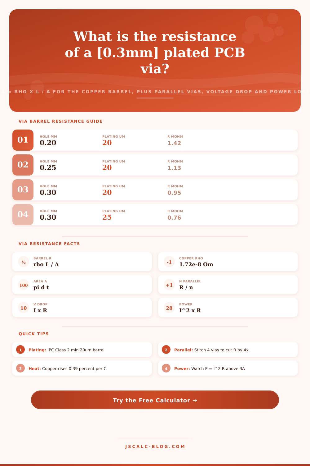
Single via, 1.6 mm board, copper at 20 C. Values in milliohms.
| Finished Hole | Plating 18 um | Plating 25 um | Plating 35 um | Reads As |
|---|---|---|---|---|
| 0.15 mm | 3.24 mohm | 2.33 mohm | 1.66 mohm | Microvia |
| 0.20 mm | 2.42 mohm | 1.75 mohm | 1.25 mohm | Fine via |
| 0.30 mm | 1.62 mohm | 1.17 mohm | 0.83 mohm | Signal via |
| 0.40 mm | 1.21 mohm | 0.87 mohm | 0.62 mohm | Medium via |
| 0.50 mm | 0.97 mohm | 0.70 mohm | 0.50 mohm | Power via |
| 0.60 mm | 0.81 mohm | 0.58 mohm | 0.42 mohm | Large via |
| 0.80 mm | 0.60 mohm | 0.44 mohm | 0.31 mohm | Heavy via |
| 1.00 mm | 0.48 mohm | 0.35 mohm | 0.25 mohm | Bus via |
📊Parallel Via Resistance Reduction
| Vias in Parallel | Combined Factor | Single = 1.0 mohm | Single = 0.5 mohm | Typical Use |
|---|---|---|---|---|
| 1 via | 1.000x | 1.000 mohm | 0.500 mohm | Signal net |
| 2 vias | 0.500x | 0.500 mohm | 0.250 mohm | Small power |
| 3 vias | 0.333x | 0.333 mohm | 0.167 mohm | Regulator out |
| 4 vias | 0.250x | 0.250 mohm | 0.125 mohm | Thermal stitch |
| 6 vias | 0.167x | 0.167 mohm | 0.083 mohm | Power plane |
| 9 vias | 0.111x | 0.111 mohm | 0.056 mohm | BGA power ball |
| 16 vias | 0.063x | 0.063 mohm | 0.031 mohm | High-current rail |
🌡Temperature Effect on Copper Resistance
| Temperature | Delta T from 20 C | Multiplier | 1.00 mohm Becomes | Note |
|---|---|---|---|---|
| 0 C | -20 C | 0.921x | 0.921 mohm | Cold start |
| 20 C | 0 C | 1.000x | 1.000 mohm | Reference |
| 25 C | +5 C | 1.020x | 1.020 mohm | Room ambient |
| 50 C | +30 C | 1.118x | 1.118 mohm | Warm board |
| 85 C | +65 C | 1.255x | 1.255 mohm | Industrial max |
| 105 C | +85 C | 1.334x | 1.334 mohm | Hot rail |
| 125 C | +105 C | 1.413x | 1.413 mohm | Automotive |
🗃Via Resistance, Drop and Loss Comparison Grid
Single-via barrel, 1.6 mm board, copper at 20 C, then the drop and loss at the listed current.
| Hole mm | Plating um | Single R | Current | V Drop | Power Loss |
|---|---|---|---|---|---|
| 0.20 | 18 | 2.42 mohm | 1 A | 2.42 mV | 2.42 mW |
| 0.25 | 20 | 1.75 mohm | 1 A | 1.75 mV | 1.75 mW |
| 0.30 | 25 | 1.17 mohm | 2 A | 2.34 mV | 4.68 mW |
| 0.40 | 25 | 0.87 mohm | 3 A | 2.61 mV | 7.83 mW |
| 0.50 | 25 | 0.70 mohm | 3 A | 2.10 mV | 6.30 mW |
| 0.50 | 35 | 0.50 mohm | 5 A | 2.50 mV | 12.5 mW |
| 0.60 | 35 | 0.42 mohm | 5 A | 2.10 mV | 10.5 mW |
| 0.80 | 35 | 0.31 mohm | 8 A | 2.48 mV | 19.8 mW |
| 1.00 | 35 | 0.25 mohm | 10 A | 2.50 mV | 25.0 mW |
⚙Formula Breakdown
💡PCB Via Design Tips
How much resistance does one plated through hole contribute to a net? This is something that tripped up many hardware designers, but there’s an answer on this page. The PCB via resistance calculator will tell you.
If you’ve ever seen vias, those little copper tubes, you’d think they were perfect conductors. They’re not. Each via add a certain amount of DC resistance. This is set by the length of the barrel, thickness of copper plating on the wall, and the resistivity of the copper itself.
Why Via Resistance Matters for Power Design
That tiny bit of resistance becomes a real voltage drop and real heat if your power rail is carrying multiple amps, so having the number matter before you commit to a board layout. All the calculations below are based off the same set of physics that applies to all conductors. The formula is: Resistance = Resistivity * Length / Cross sectional Area. In other words, R = rho * L / A.
The resistivity rho in the case of a via is the resistivity of plated copper (about 1.72 times 10 to the minus 8 ohm-metres at twenty degrees Celsius). The length L is length of the barrel of the via, i.e., how far the via has to pass through the board (usually around 1.6 mm for a typical four layer board).
This leaves the area A as the problem, since it is not the entire area of the hole that current flows through, just the area of the plated copper on its walls. Most estimates miss this point. The via barrel is a hollow copper cylinder. A cross section of that cylinder is called an “annular ring“: the outer circle minus the inner hole. Using the finished hole diameter di and the plating thickness t, the outer diameter is do = di + 2t (because plating coats both sides of the wall). The actual copper area is pi divided by four times difference of squared diameters. When the wall thickness is as thin as in real boards, this simplifies to a slightly better but still fairly simple approximation. The area A is about pi times d times t. A hole of 0.3 mm with twenty-five microns of plating has just about 0.024 square millimetres of copper, so you can see why it isn’t zero resistance and matters for high-current paths.
A note on copper resistance and temperature
Since copper’s a positive-temperature-coefficient conductor, that means it increase in resistance when heated. It’s an important factor for design accuracy; knowing what direction things are going will prevent any surprises. After you put your operating conditions into the calculator (above), it’ll spit out the number for you, but know the trend: copper has an alpha of 0.00393 per degree Celsius. Translation: For each degree over 20 degrees celsius, your copper gets around 0.39 percent more resistive. So at an industrial junction temperature of eighty five degrees celsius, the barrel will have a resistance 1.26 times higher than at room temperature. Voltage drop and therefore power loss scale with resistance, so if you ignore temperature you might well be underestimating losses on a hot rail significantly.
A few other rules: Using multiple vias in parallel (which is like making an array) reduces resistance to 1/nth of the resistance of a single via. That’s why they make those big arrays of vias under the power balls of a BGA and stitch arrays of thermal vias under hot components. It’s also why the fastest way to reduce your via resistance is with some number of vias in parallel. You can see from table on the page how fast resistance drops as you add more paths in parallel, which means it’s far less expensive to drill multiple smaller holes than trying to find some magical huge hole for current to travel through.
From these figures, you have two additional instant results from simple circuit laws. The voltage dropped across those vias is V equals I times R (i.e., current multiplied by the total resistance). The heat that’s dissipated is P equals I squared times R, rising with the square of the current. With a 2 amp draw through a 0.6 milliohm via path, only 1.2 mV is dropped and only 2.4 mW is burned, which is insignificant. Increase it to ten amps and the drop rise to 6 mV while the power leaps to 60 mW, all focused into an extremely small volume of copper. It’s that localized heating that leads us to the need for sufficient plating on a high-current design, along with the use of parallel vias.
Resistances of a milliohm in vias are generally unimportant on signal nets. This is not true for power distribution. Series via resistance dumps heat into the board, eats into the tolerance of a tightly regulated rail, and adds directly to IR drop budgets. This makes a regulator feeding a processor through under-sized vias sag below spec under load. Additionally, a thermal via field that is too sparse can allow a power stage to run hot.
This tool puts the drop and loss, barrel resistance formula, temperature correction and parallel combination all in one place. Once you start from a preset, adjusting for your actual geometry and current allows you to design your power path with confidence and ensure those tiny copper tubes don’t overheat or sag while doing their job.