PCB Trace Width Calculator
Find the required copper trace width for a given current using the IPC-2221 standard. Enter your current, copper weight, allowable temperature rise and layer type, and the tool returns the minimum trace width in mils and millimeters, the cross-sectional area, and the resulting resistance and voltage drop over your trace length.
🔌Real Design Presets
📝Trace and Current Inputs
Continuous current the trace must carry, in amperes.
Finished copper thickness of the layer, in ounces.
Outer traces cool better, so they need less width.
Trace heating above ambient, typically 10 to 30 °C.
Board surroundings; sets the final conductor temperature.
Conductor run length, used for resistance and voltage drop.
Resistivity used for the resistance calculation.
Controls rounding on every result card.
🔢Formula Snapshot
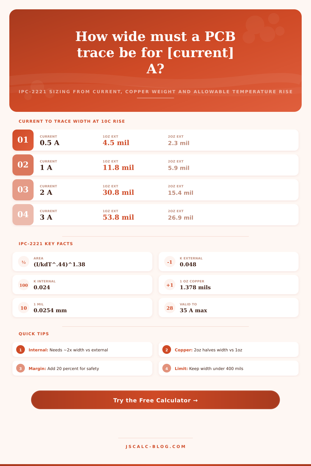
📋Current to Width, 1oz External at 10°C Rise
| Current | Area (mils²) | Width (mils) | Width (mm) |
|---|---|---|---|
| 0.5 A | 6.3 | 4.5 | 0.11 |
| 1 A | 16.3 | 11.8 | 0.30 |
| 2 A | 42.4 | 30.8 | 0.78 |
| 3 A | 74.2 | 53.8 | 1.37 |
| 5 A | 150.0 | 108.9 | 2.77 |
| 7 A | 238.6 | 173.2 | 4.40 |
| 10 A | 390.3 | 283.2 | 7.19 |
| 15 A | 682.8 | 495.5 | 12.59 |
📊Copper Weight to Thickness Reference
| Copper Weight | Thickness (mils) | Thickness (µm) | Typical Use |
|---|---|---|---|
| 0.5 oz | 0.689 | 17.5 | Fine-pitch signal |
| 1 oz | 1.378 | 35 | General purpose |
| 2 oz | 2.756 | 70 | Power and heavy current |
| 3 oz | 4.134 | 105 | Motor drives, bus bars |
| 4 oz | 5.512 | 140 | High-current backplanes |
| 0.25 oz | 0.345 | 8.75 | RF and dense routing |
📏Unit Conversions
| Unit | Equals | In Base Unit | Note |
|---|---|---|---|
| 1 mil | 0.0254 mm | 0.001 inch | One thousandth of an inch |
| 1 mm | 39.37 mils | 0.03937 inch | Metric width |
| 1 oz copper | 1.378 mils | 35 µm | Standard 1 oz layer |
| 1 mil² | 0.000645 mm² | 645.16 µm² | Area conversion |
| 1 A | 1000 mA | 1 C/s | Ampere of current |
| 1 Ω | 1000 mΩ | 1 V/A | Ohm of resistance |
🗃External vs Internal Width Comparison Grid
| Current | 1oz Ext (mils) | 2oz Ext (mils) | 1oz Int (mils) | 2oz Int (mils) | Area (mils²) |
|---|---|---|---|---|---|
| 0.5 A | 4.5 | 2.3 | 11.8 | 5.9 | 6.3 / 16.3 |
| 1 A | 11.8 | 5.9 | 30.8 | 15.4 | 16.3 / 42.4 |
| 2 A | 30.8 | 15.4 | 80.4 | 40.2 | 42.4 / 110.8 |
| 3 A | 53.8 | 26.9 | 140.5 | 70.3 | 74.2 / 193.7 |
| 5 A | 108.9 | 54.4 | 284.3 | 142.1 | 150.0 / 391.7 |
| 7 A | 173.2 | 86.6 | 452.2 | 226.1 | 238.6 / 623.1 |
| 10 A | 283.2 | 141.6 | 739.5 | 369.7 | 390.3 / 1019 |
| 15 A | 495.5 | 247.7 | 1294 | 647 | 682.8 / 1783 |
| 20 A | 736.8 | 368.4 | 1924 | 962 | 1015 / 2651 |
| 25 A | 1002 | 501.2 | 2617 | 1309 | 1381 / 3607 |
⚙Formula Breakdown (IPC-2221)
💡PCB Trace Design Tips
Then again, you get the board back and discover the power rail melted before the thing powered up. Nobody wants to admit how often that happens. Copper traces appears as thick wire in CAD view, but they are actualy thin sheets of metal with exact thermal limits. Getting the trace size right isn’t an act of guesswork, or at least not most of the time, it’s an exercise in understanding how much heat needs to dissipating for the current you want to run through it.
Fortunately the tool on this page handles the heavy lifting by applying IPC-2221 standard for you, so you just need to check if computed width works within your design instead of fighting with constants and exponents.
How to Size Copper Traces Correctly
Here’s the problem: Heat is a side effect of electrical resistance. As electrons move along a narrow surface, they bump into individual copper atoms and convert some electrical energy into heat. Unless the heat dissipates quickly enough, this cause the trace to become hotter. And that’s problematic because heat can damage nearby circuit element or cause the board substrate itself to peel apart.
The calculator calculates the required width based on amount of current you require and the temperature rise you are willing to tolerate. Then it provides you with a width value that strikes best balance between these two factor. Designers who don’t use thermal information and rely only on visual estimation gets this wrong.
Two primary constants in this equation mirror laws of physics: A trace laid down on an outside layer of a board has direct exposure to ambient temperature and dissipates heat easily, needing only 1/4 the cross section as one routed internally which is sandwiched between layers of insulating material and thus traps heat within the board. This is why you’ll note that internal power plane traces is often thicker copper, or have larger traces. This is reflected in the math, it calls for about 2.5x the surface area of copper for internal traces. When you choose your layer type, the calculator will factor this in for you (so don’t forget and undervolt a hidden rail!)
The other variable that changes the game is the kind of copper used. Normal 1 oz copper comes in at around 35 micrometers thick. But if you use 2 oz copper then you get twice as thick without having to make it any wider. Since resistance depends on cross-sectional area, you can cut the trace width in half and still carry same current. When you’re working with limited board space, this is an extremely valuable trade off. Maybe there’s no room for a wide power rail, but you can always specify heavier copper with your manufacturer. With the tool, you can step from 0.5 oz all the way to 3 oz. This lets you visualize amount of space you’ll be able to save by upgrading material thickness.
Power distribution’s silent killer is its own voltage drop. Sure, a trace may not heat up but that doesn’t mean it isn’t electrically failing by dropping too much voltage en route to the load. Too much resistance in path back to the regulator means a starving sensor readout or processor core. With the resistivity of copper as a variable (not constant!), the calculator bases the voltage drop based off your inputted trace length. It then presents you with a concrete number in millivolts so that you know whether to go for a shorter route or a wider trace. This transforms an abstract thermal limit into real electrical performance measure.
There are no perfect manufacturers in the real world so there will be margins added for real world designs. Traces etched will be slightly smaller than they was drawn. Localized resistances of vias and pads aren’t included in basic linear calculations. Add another 20% to your designed width for good measure. That accounts for not only tolerances but also ambient variation and heating up of connectors. So the final design is solid instead of being right on the edge of failing. You should of added more just in case.
Using presets can speed up your workflow by providing realistic starting points. The presets are realistic starting points, which means they accelerate your work flow. Quickly seeing what a 20 A battery bus looks like versus a 1 A signal line saves retyping numbers each time. This also shows the size difference between heavy power lines and delicate logic wires. Then you adjust variables to fit conditions on your boards.
It is a little thing, but it makes all the difference when it comes to reliability. After all, you want a board that runs cool under load and provides stable voltage. The calculator provides the data to do just that; engineering, not guesswork.