Junction Temperature Calculator
Predict the semiconductor junction temperature Tj from power dissipation, ambient temperature and the thermal resistance stack. Use a single junction-to-ambient value or the full junction-to-case, case-to-sink and sink-to-ambient path to also get case temperature, temperature rise, the margin to the rated Tj max, and the maximum power the design can safely handle.
⚡Choose a Thermal Path
🎯Real Design Presets
🔥Thermal Inputs
Heat the device turns into thermal power, in watts.
Air temperature around the part, not room temperature.
Simple path: total resistance from junction to air.
Internal die to package case, from the datasheet.
Thermal interface material and mounting, grease or pad.
Heatsink resistance to air at the chosen airflow.
Absolute maximum Tj from the device datasheet.
Target ceiling used for the pass or fail check.
Controls rounding on every result card.
🔢Formula Snapshot
📋Power and Theta-JA to Tj Examples
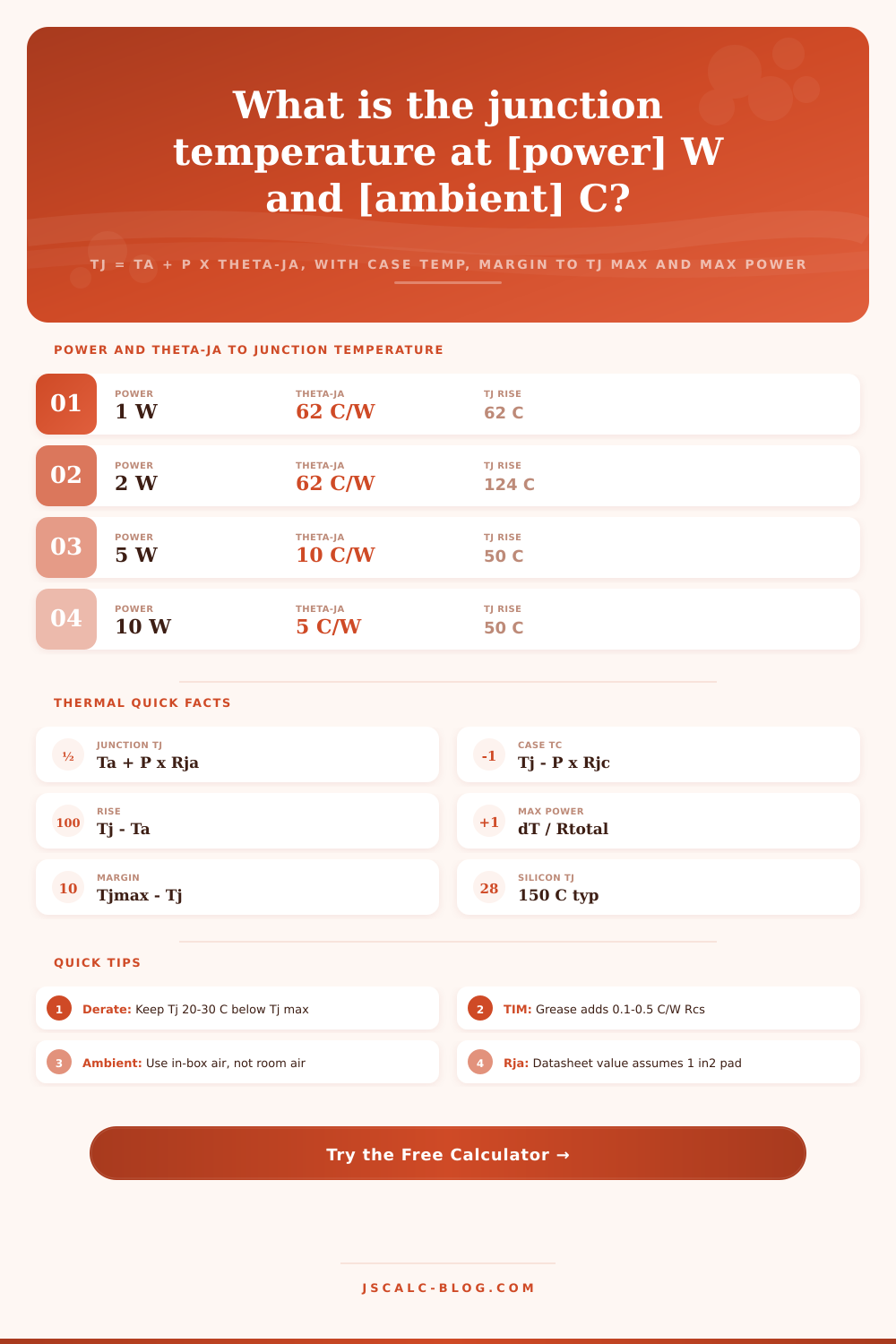
| Power P | Theta-JA | Rise P x Rja | Tj at 40 C Ambient |
|---|---|---|---|
| 0.5 W | 200 C/W | 100 C | 140 C |
| 1 W | 62 C/W | 62 C | 102 C |
| 1 W | 150 C/W | 150 C | 190 C over limit |
| 2 W | 62 C/W | 124 C | 164 C over limit |
| 3 W | 20 C/W | 60 C | 100 C |
| 5 W | 10 C/W | 50 C | 90 C |
| 8 W | 6 C/W | 48 C | 88 C |
| 10 W | 5 C/W | 50 C | 90 C |
| 15 W | 3 C/W | 45 C | 85 C |
| 25 W | 2 C/W | 50 C | 90 C |
📊Device Max Tj and Package Theta-JC Grid
| Device Type | Package | Typical Tj Max | Theta-JC | Theta-JA Free Air | Notes |
|---|---|---|---|---|---|
| Silicon signal IC | SO-8 | 150 C | 40 C/W | 120 C/W | Small die |
| Silicon linear reg | TO-220 | 150 C | 3 C/W | 62 C/W | Tab mount |
| Power MOSFET | D2PAK | 175 C | 1.0 C/W | 40 C/W | Surface tab |
| Power MOSFET | TO-247 | 175 C | 0.5 C/W | 40 C/W | Large tab |
| Schottky diode | SOT-223 | 150 C | 15 C/W | 53 C/W | Copper pour |
| IGBT module | Module | 150 C | 0.25 C/W | Sink only | Baseplate |
| High-power LED | Star MCPCB | 125 C | 4 C/W | 30 C/W | Junction Tj |
| LED COB array | COB panel | 120 C | 0.8 C/W | Sink only | Large emitter |
| CPU or SoC | BGA + IHS | 100 C | 0.2 C/W | Cooler only | Tj max low |
| GaN transistor | QFN | 150 C | 1.5 C/W | 50 C/W | Fast switch |
🧩Thermal Interface Material Theta-CS Guide
| Interface Method | Typical Theta-CS | Best Use | Note |
|---|---|---|---|
| Bare metal, dry | 0.5 - 1.0 C/W | Rough contact | Air gaps hurt |
| Thermal grease | 0.1 - 0.5 C/W | Most power parts | Thin even layer |
| Silicone pad | 0.4 - 1.2 C/W | Isolation needed | Adds Rcs |
| Mica + grease | 0.6 - 1.4 C/W | High voltage | Electrical isolate |
| Graphite sheet | 0.1 - 0.3 C/W | Clean reusable | No pump-out |
| Phase change pad | 0.1 - 0.4 C/W | Production CPU | Melts on heat |
📏Thermal Resistance Unit Reference
| Symbol | Meaning | Unit | Note |
|---|---|---|---|
| Rja | Junction to ambient | C/W | Full simple path |
| Rjc | Junction to case | C/W | Inside package |
| Rcs | Case to sink | C/W | Interface layer |
| Rsa | Sink to ambient | C/W | Heatsink to air |
| P | Power dissipated | W | Heat generated |
| Tj | Junction temp | C | Die temperature |
⚙Formula Breakdown
💡Junction Temperature Design Tips
One of the questions you have when designing with power electronics is answered by this: How hot does my silicon actualy get? All those LEDs, regulators, transistors, diodes. They all convert power to heat in a junction somewhere inside them. That junction cannot exceed its rated value or else it will fail (or just degrade).
Given three values you can either lookup or measure, this tool calculates the junction temperature. It tells you case temperature and how much that rises above ambient. It also shows whether there’s any margin left before failure and maximum amount of power the design can support.
Calculate How Hot Your Electronic Parts Get
A junction is where current flows, and it is the active part of semiconductor die. Because it is inside a package, you do not normally measure junction temperature directly but instead derive it from heat flow path. Heat flows out of the junction then out of the package and into the case. It moves through some thermal interface into a heatsink then spreads into surrounding air. At each point it is resisted by something, and those things are measured in degrees celsius per watt.
The governing relationship is the ambient temperature plus power times total thermal resistance. One of these numbers (the fastest) is labeled theta-JA. That’s the junction-to-ambient thermal resistance. If you’ve seen datasheets, you know they quote this for their typical test board. For example, a TO-220 in free air might be 62 C per watt. For example, a small surface-mount package with no heatsink can be well over 100 C per watt.
Plug in your power, the ambient temperature, and that number to see the math predict the die temperature. For parts without heatsinks, or for an initial check, this quick route works great. Even if you’re running a one-watt part on a very high-resistance package at forty degrees ambient, the heat can add up fast.
Adding a heatsink requires more data. No longer will a single number do. You now need the entire stack of resistances. Now we have to calculate junction-to-case + case-to-sink + sink-to-ambient for a total resistance. These is resistances in series, just like electrical resistors. Reducing any of these reduces the junction temperature.
Plug in those individual path resistances into the calculator and it does all that math for you. That way you don’t forget about the interface layer and then sum the stack wrong, which saves you from having to manually sum the resistances yourself. And it opens up case temp by subtracting the internal drop from the junction temp. Those in-between temps enables checking a design against a sink or tab thermocouple readout.
All calculations are filled out onto four result cards, providing a complete view. The headline number is on the junction temperature card. Beneath that is the rise over ambient. Case temperature card presents the package surface you can stick a probe into. Temperature rise card isolates the self-heating. This is the bit of temperature you get to control via design change.
And finally, the margin card shows how far there is to go to the absolute maximum. What is the maximum power the stack can dissipate before it hits its target ceiling? The lowest bar here (the min) is not your goal, but rather just a minimum. For semiconductors, every ten degree drop in junction temperature roughly doubles their life.
That’s why seasoned designers derate. They choose a target closer to 80% of their rating. That provides insurance against both electromigration on the bond wires and thermal stress. You can set this ceiling in the tool. If you’re getting dangerously close, it will flag the design.
To predict well, use true values for inputs. From the device’s datasheet you get maximum ratings and junction-to-case resistance. Those is typically reliable. For case-to-sink resistance, your interface dictates things. With dry metal contact, that value can be as high as one degree per watt. Thermal grease drops it significantly. Somewhere in the middle lies an insulating silicone pad.
Next comes sink-to-ambient which comes from the heatsink datasheet assuming the stated airflow. That leaves ambient temperature, perhaps the most difficult input. Fifteen to twenty-five degrees above room temp is typical for the air adjacent to the part within a sealed box. A common misstep is using room temp rather than actual in-box ambient. It can hide a thirty degree error in the predicted junction.
It’s fast because the tool comes pre-loaded with presets from typical hardware scenarios. Load a five-watt linear regulator with a heatsink in place. Load a surface mount two-watt part without a heatsink. Or maybe you have a high-power LED array? Each preset loads up a complete set of realistic values. It recalculates on-the-fly so that you can see how heatsink size, interface quality, and package choice move the needle. Pick the closest-to-your-part preset to start with. Tweak the resistances or powers to match what you actualy have.
Intermittent thermal failures are expensive. Thermal failure happens when a product gets hot in the field. The failure shows up intermittently. Thermal failures are expensive and often intermittent, showing up only when a product runs hot in the field. You don’t know until it’s too late.
This calculator takes a known thermal stack and predicts the die temperature, case temp, rise, margin, and max power. With this calculator, it takes seconds of arithmetic to check your design instead of guessing whether or not your heatsink will be big enough. It should of been cheap insurance that your silicon isn’t going to cook when you build hardware. Your designs stays cool and your silicon stays alive.