FLOPS Calculator
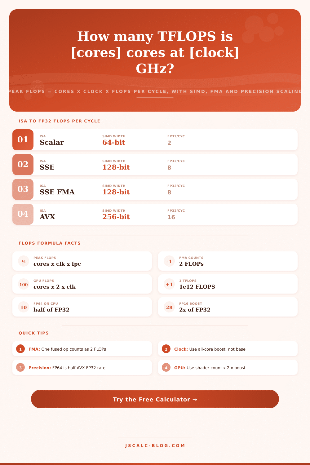
Estimate theoretical peak floating-point throughput from cores times clock times FLOPs per cycle. Choose a CPU SIMD ISA such as AVX2 or AVX-512, or switch to GPU mode using shaders times two for the fused multiply-add, then scale by FP16, FP32, or FP64 precision and multiply across every socket or GPU to read GFLOPS, TFLOPS, and the FP64 rate.
🖥Choose a Compute Type
🎯Real CPU and GPU Presets
📝Hardware Inputs
Physical cores that run the SIMD units.
Total FP32 lanes across all streaming units.
All-core boost clock in GHz, not the base clock.
FMA is fused multiply-add, so it counts as 2 FLOPs.
Enter FLOPs per cycle directly if ISA is Custom.
Sets the main result rate relative to FP32.
Fraction of FP32 throughput available at FP64.
Number of identical CPUs or GPUs in the system.
🔢Formula Snapshot
📋FP32 FLOPs per Cycle by ISA
| Instruction Set | SIMD Width | FP32 per Cycle | Notes |
|---|---|---|---|
| Scalar x87 / SSE1 | 32 to 128-bit | 2 | 1 add + 1 mul or FMA |
| SSE2 to SSE4 + FMA3 | 128-bit | 8 | 4 lanes, mul and add |
| AVX (no FMA) | 256-bit | 16 | 8 lanes add and mul |
| AVX2 + FMA3 | 256-bit | 16 | 8 lanes fused per port |
| AVX-512 single FMA | 512-bit | 32 | 16 lanes fused |
| AVX-512 dual FMA | 512-bit | 64 | Two 512-bit FMA ports |
| Arm NEON + FMA | 128-bit | 8 | 4 lanes, Apple and Arm |
| Arm SVE2 256-bit | 256-bit | 16 | Server scalable vectors |
📊Precision Scaling Factors
| Precision | Bits | CPU vs FP32 | Consumer GPU | Data-Center GPU |
|---|---|---|---|---|
| FP16 half | 16-bit | 2x (with support) | 1x to 2x | 2x to 4x |
| BF16 brain float | 16-bit | 2x | 1x to 2x | 2x to 4x |
| FP32 single | 32-bit | 1x baseline | 1x baseline | 1x baseline |
| TF32 tensor | 19-bit | not native | varies | up to 8x tensor |
| FP64 double | 64-bit | 1/2 | 1/16 to 1/32 | 1/2 |
📏FLOPS Unit Scale
| Unit | Symbol | FLOPS | Typical Example |
|---|---|---|---|
| Kiloflops | kFLOPS | 1e3 | 1960s early computers |
| Megaflops | MFLOPS | 1e6 | 1980s workstations |
| Gigaflops | GFLOPS | 1e9 | Single desktop core |
| Teraflops | TFLOPS | 1e12 | Modern GPU or CPU |
| Petaflops | PFLOPS | 1e15 | Large GPU cluster |
| Exaflops | EFLOPS | 1e18 | Frontier-class systems |
🗃Real CPU and GPU Peak FLOPS Comparison
| Chip | Type | Cores / Shaders | Clock | FP32 per Cycle | Peak FP32 |
|---|---|---|---|---|---|
| Ryzen 9 7950X | CPU AVX2 | 16 | 4.5 GHz | 16 | ~1.15 TFLOPS |
| Core i9-13900K | CPU AVX2 | 24 | 3.9 GHz | 16 | ~1.5 TFLOPS |
| Xeon Platinum 8480 | CPU AVX-512 | 56 | 2.9 GHz | 64 | ~10.4 TFLOPS |
| EPYC 9654 | CPU AVX-512 | 96 | 3.55 GHz | 32 | ~10.9 TFLOPS |
| Apple M2 Max | CPU NEON | 12 | 3.68 GHz | 8 | ~0.35 TFLOPS |
| RTX 4090 | GPU FP32 | 16384 | 2.52 GHz | 2 | ~82.6 TFLOPS |
| RX 7900 XTX | GPU FP32 | 6144 | 2.5 GHz | 2 | ~61.4 TFLOPS |
| NVIDIA A100 | GPU FP64 | 6912 | 1.41 GHz | 2 | ~19.5 FP32 TFLOPS |
| NVIDIA H100 SXM | GPU FP32 | 16896 | 1.98 GHz | 2 | ~67 TFLOPS |
| Threadripper 7980X | CPU AVX-512 | 64 | 3.2 GHz | 32 | ~6.6 TFLOPS |
⚙Formula Breakdown
💡FLOPS Estimation Tips
If you’ve seen marketing materials from contemporary processors, chances are you saw a lot about core count and clock speed. Those aren’t interchangeable units of processing power. A processor with fewer instructions and a very fast clock speed will often perform worse than a processor with a wider vector width and a slower clock. Floating point operations per second (FLOPS) are the best direct measurement of raw computing power. Why? Because it takes into account all variables without cherry-picking what looks good.
How many cores? How fast do those cores spin? And how much can a given core gets done during each clock cycle? Hype be damned. Here’s the simple formula for theoretical peak FLOPS. Take the frequency in hertz and multiply it by the number of parallel execution units. Multiply again by the number of FLOPs they completes each cycle. This last bit is where most people get tripped up.
The Real Way to Measure Computer Power
More cores isn’t everything. You also need to account for what your cores are doing. Today’s processors use SIMD, which stands for single instruction multiple data, to process information in vectors. They process a vector of numbers simultaneously. An AVX2 256-bit register contains eight thirty-two-bit floats. Every lane gets hit with one instruction. Small features of architecture have huge impacts. One such feature is called Fused Multiply-Add, or FMA. It do a multiply-and-add in a single operation, meaning it’s two floating-point operations.
One instruction touches all eight AVX2 lanes. Multiply that times two (operations) and you get sixteen FP32 FLOPs out of a single core, per cycle. That’s eight using narrower SSE instructions. AVX-512 has a wider lane count of thirty-two. For servers, double the number of FMA units and we’re at sixty-four.
Plug all this into calculator, and it will do the math for you. No need to remember coefficients; it shows why wider vectors are useful. For servers, double the number of FMA units and we’re at sixty-four. Plug all this in the calculator, and it will do the math for you. No need to remember coefficients; it demonstrates value of wider vectors.
The same idea applies for graphics processors, though they do things differently. A GPU consists of thousands of tiny shader core, while a CPU typically has a couple dozen wider cores. Since each shader core can executes an FMA every cycle, the equation is: (shader count x 2) x clock frequency. With more than sixteen thousand shaders operating near 2.5 GHz on an RTX 4090, that’s more than eighty teraflops of peak single-precision performance. On the GPU side, we swap out the core count for a shader count and tweak the per-lane number so it matches up. That way, you don’t have to plug numbers into a calculator and hope your math was right to get a meaningful comparison between a gaming card and a server CPU.
All else is secondary to precision. Double precision is the pricey choice; double precision on consumer gaming cards can be throttled down to a fraction (sometimes as low as 1/32), since most games don’t need that amount of accuracy. FP64 on data center CPUs and GPUs will usually run at half the speed of FP32. Single precision is the workhorse. Half precision at sixteen bits often runs twice as fast because two numbers fit into the space one would otherwise take up. The tool separates out this double-precision speed and puts it in its own result card, which is key if you’re not rendering frames but rather running some sort of scientific simulation.
All FLOPS numbers come with one honest caveat. The number generated above is a theoretical peak. That means we assume there are no memory bottlenecks. We also assume there are no cache misses or stalls. Finally, we assume each core spits out a full vector once a cycle. Of course, real workloads don’t hit that ceiling. Well-tuned benchmark code may reach seventy to ninety percent of the peak. And ordinary code will run much lower because it is limited by something other than the ability to do math, usually bandwidth. So think of the peak value as an upper bound but not a guarantee.
Use a preconfigured spec like the Ryzen 9 7950X to see what a familiar set of specs decomposes into in terms of clock speed, cores, and FLOPs per cycle. Now adjust them one at a time. Double the clock? Yes, peak doubles. Change from single to double precision? Yes, the rate drops. Need an answer for your render farm size, or wondering how your spec sheet breaks down into teraflops? This clear calculation provides an answer based off the simple fact of multiplying cores by clock speed and operations per cycle.
You should of used this before.