Decoupling Capacitor Value Calculator
Size the bypass capacitor for a digital IC three ways: the charge-transfer method C = (dI x dt) / dV that holds the rail droop under a transient, the target-impedance method C = 1 / (2 pi f Z) with Z = dV / dI, and the classic rule of thumb of one 100nF ceramic per power pin plus a bulk cap. Every result snaps to the nearest standard E-series capacitor value.
⚡Choose a Sizing Method
📌Real Decoupling Presets
🔧Decoupling Inputs
Peak switching current the IC pulls in a burst.
Max rail dip you will tolerate during the transient.
How long the current transient lasts, in nanoseconds.
Nominal supply pin voltage, used for droop percent.
Highest frequency the cap must hold Z below.
Applies to the target impedance frequency above.
Rule of thumb places one ceramic per power pin.
Local high-frequency cap fitted at each pin.
Larger tank cap shared across the device rail.
Equivalent series resistance for the ESR droop card.
🔢Formula Snapshot
📈Transient to Capacitor Value
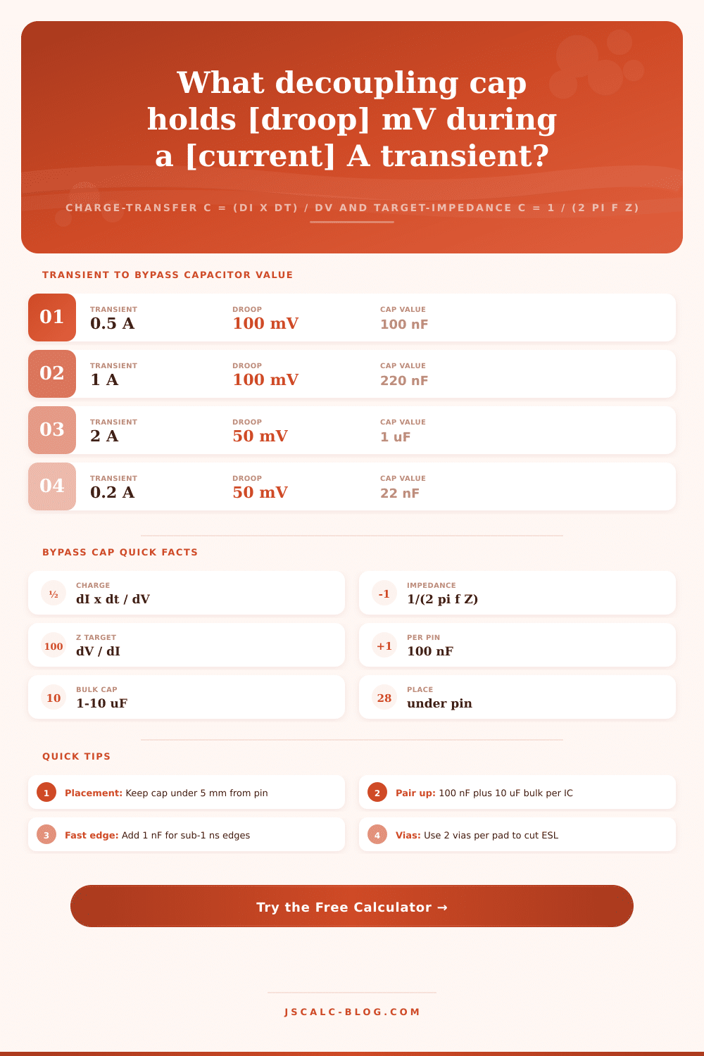
| Transient dI | Droop dV | Transition dt | C = dI dt / dV | Standard Cap |
|---|---|---|---|---|
| 0.5 A | 100 mV | 20 ns | 100 nF | 100 nF |
| 1 A | 100 mV | 20 ns | 200 nF | 220 nF |
| 1 A | 50 mV | 20 ns | 400 nF | 470 nF |
| 2 A | 50 mV | 25 ns | 1.0 uF | 1 uF |
| 0.2 A | 50 mV | 10 ns | 40 nF | 47 nF |
| 3 A | 100 mV | 15 ns | 450 nF | 470 nF |
| 0.1 A | 50 mV | 5 ns | 10 nF | 10 nF |
| 5 A | 50 mV | 40 ns | 4.0 uF | 4.7 uF |
📡Target Impedance Method Chart
| Droop dV | Transient dI | Z = dV / dI | Frequency f | C = 1/(2 pi f Z) |
|---|---|---|---|---|
| 50 mV | 1 A | 50 mOhm | 1 MHz | 3.2 uF |
| 50 mV | 1 A | 50 mOhm | 10 MHz | 318 nF |
| 100 mV | 2 A | 50 mOhm | 20 MHz | 159 nF |
| 100 mV | 1 A | 100 mOhm | 50 MHz | 32 nF |
| 30 mV | 0.5 A | 60 mOhm | 100 MHz | 27 nF |
| 25 mV | 1 A | 25 mOhm | 1 MHz | 6.4 uF |
| 20 mV | 2 A | 10 mOhm | 5 MHz | 3.2 uF |
🔧Rule of Thumb by IC Type
| Device | Rail | Per Pin Ceramic | Bulk Cap | Notes |
|---|---|---|---|---|
| 8-bit MCU | 3.3 V / 5 V | 100 nF | 1-10 uF | One per Vdd pin |
| Logic gate | 5 V TTL | 100 nF | 10 uF / row | One per package |
| Op-amp | +/- 5 V | 100 nF | 1 uF | Both rails |
| FPGA core | 1.0-1.2 V | 100 nF x many | 10-100 uF | Plus 1 nF HF |
| DDR memory | 1.5 V | 100 nF + 10 nF | 22 uF | Very short loop |
| ADC / DAC | 1.2-3.3 V | 100 nF | 10 uF | Split analog rail |
| RF front end | 1.8-3.3 V | 100 pF + 1 nF | 1 uF | Smallest package |
📏Standard Capacitor Value Ladder
| Value | In Farads | Reads As | Typical Use |
|---|---|---|---|
| 1 nF | 0.000000001 F | 1000 pF | RF / fast edge |
| 10 nF | 0.00000001 F | 0.01 uF | Fast logic HF |
| 100 nF | 0.0000001 F | 0.1 uF | General bypass |
| 1 uF | 0.000001 F | 1000 nF | Small bulk |
| 10 uF | 0.00001 F | 10000 nF | Bulk reservoir |
| 100 uF | 0.0001 F | 100000 nF | Board input |
🗃Method Comparison Grid
| Scenario | dI | dV | dt / f | Charge C | Impedance C | Standard |
|---|---|---|---|---|---|---|
| MCU 3.3V | 0.5 A | 100 mV | 20 ns | 100 nF | 16 nF | 100 nF |
| Logic 5V | 1 A | 100 mV | 20 ns | 200 nF | 32 nF | 220 nF |
| Op-amp 5V | 0.3 A | 50 mV | 15 ns | 90 nF | 27 nF | 100 nF |
| FPGA core | 3 A | 50 mV | 10 ns | 600 nF | 95 nF | 680 nF |
| DDR3 1.5V | 2 A | 50 mV | 5 ns | 200 nF | 64 nF | 220 nF |
| ADC 1.2V | 0.2 A | 25 mV | 20 ns | 160 nF | 13 nF | 220 nF |
| CPU 1.0V | 5 A | 50 mV | 8 ns | 800 nF | 159 nF | 1 uF |
| RF 2.4GHz | 0.1 A | 30 mV | 1 ns | 3.3 nF | 0.1 nF | 3.3 nF |
⚙Formula Breakdown
💡Practical Layout Tips
Digital boards glitch or run clean when loaded. Depending on which decoupling capacitor you choose for them. When an FPGA or microcontroller changes state, it grabs a quick pulse of current off its power pin. That is too much for the primary power supply and its traces to handle quickly. If they don’t get a cap nearby to immediately give them the juice, rail voltage will droop. This calculator will size that bypass cap in one of three methods: pick the best fit for how your circuit works. No guesswork needed; only concrete part numbers resulting from abstract needs.
Decoupling capacitors is little local energy reservoirs located next to each power pin on an integrated circuit. Regulators have a limited response time and the traces leading up to the IC has some inductance. Without such a capacitor, supply voltage to the chip would dip when the chip pulls a sudden current spike. This supply droop causes the rail to fall below the minimum operating voltage and potentially result in resets and other logic errors. By supplying that burst of charge from millimeters away, it holds the rail within tolerance. Lower-inductance caps that are also close perform the task better. Why? Trace inductance makes a perfect capacitor into a useless antenna at high frequency, so distance matters.
How to Choose Decoupling Capacitors
To size a bypass capacitor directly, start with amount of charge a transient requires. The transient asks for roughly Q = dI times dt. That’s the amount of charge you need to pull from the capacitor if the load current changes during a switch time of dt seconds by an amount dI. Then the capacitor has to be large enough so its capacitance C satisfies: C = (dI x dt) / dV, where dV is how much voltage droop you can tolerate. So if I have a 1 A transient coming on for 20 ns, and I don’t want my voltage to droop past 100 mV, then I need approximately 200 nF. It’s a straight-forward calculation tied directly to the physical reality of a burst of charge being limited in how far it can drop the voltage. You plug your particular case of current spike and timing sensitivity into this and result is the smallest capacitors needed at that instant.
Instead of worrying about a single transient, high-speed designers prefer to think in terms off the impedance of their power delivery network. The concept goes like this: the rail can tolerate an impedance no larger than the allowable droop divided by the transient current, which means the target impedance is Z = dV / dI. If your maximum droop is 50 mV and your transient current is 1 A then the ceiling impedance is 50 milliohms. You want a cap whose reactance stays below that ceiling out to some frequency f; to calculate how big capacitor needs to be, do C = 1 / (2 pi f Z). Why is this such a powerful view? Because it prompts us to use multiple caps in parallel to smooth the impedance over a broad frequency range. It’s a shift from “can I survive this one hit” to “how stable am I across this spectrum of noise”.
But not all designs need a detailed calculation. Years of experience has boiled down a safe default where every digital IC gets one 100 nF ceramic capacitor at each of its power pins, plus a slowish (1 to 10 uF) bulk capacitor as a reservoir. The former deals with those rapid switching edges. The latter refuels the little capacitors when nothing big is happening and keeps the voltage steady for lower frequency demands. You extend that into multiple values in parallel if it’s a densely packed part (like an FPGA), and maybe include a 1 nF just in case there’s anything faster than the 100 nF can handle. That way you know how much you’ve got on any given rail at a glance, thanks to rule-of-thumb mode. It’s a safety net that catches designs before they go too far wrong.
The formula never quite gets you onto a purchaseable value. They make capacitors in standard ladders like this: 1 nF, 10 nF, 22 nF, 47 nF, 100 nF, 220 nF, 470 nF, 1 uF, 4.7 uF, and 10 uF. So what comes out the other side of the calculator is rounded up to the next nearest value so that it’s an actual thing you can add to your bill of materials. This provides a small safety margin because choosing a higher value instead of a lower one means the capacitor is larger, but it keeps the droop closer to the minimum required by the math. This is where most folks goes wrong trying to get optimal cost: they want to pick the next smaller available value.
But no, they aren’t perfect. They have equivalent series inductance (ESL) and equivalent series resistance (ESR), both of which are bad traits in any component. As soon as there’s current flowing, that ESR introduces an immediate voltage step proportional to ESR times dI. This means a 1 A transient across 30 milliohms causes a 30 mV jump before the cap even does anything about it. This explains why you want low-ESR multilayer ceramic caps for your tight rails, and why the calculator shows the ESR droop separately on its set of results cards. And above a given cap self-resonant frequency, the ESL dominates and the cap starts looking inductive, that’s what really makes the loop length and placement more important than absolute value of capacitance at higher frequencies.
For example, picking a slightly larger capacitor than needed is better because it provides a small safety margin and holds the droop tighter. Inductance increases quickly based off length. The loop between the capacitor, the IC pins it plugs into, and the via connections has some inductance. If those paths are long, they will increase your effective ESR and ESL. Best: place the bypass cap within a few millimeters from the power pin, mount using 2 vias per pad (reducing mounting inductance by about half), and make sure ground return goes right under the component. Multiple capacitors in parallel of equal values will reduce their combined ESL and ESR; sometimes that’s better than just having a larger single capacitor.
Visit JSCalc-Blog.com for more design references and testing tools. They’re not in competition; they complement each other. Apply the rule of thumb for quick estimates and wherever the datasheet itself says it’s good to add decoupling. Grab the charge-transfer formula when you have an estimate of the transient current (and how long it lasts) and need an answer you can back up. Use the target-impedance method for high-speed rails where you need a flat power delivery network over a broad range. Begin with one of the included presets, tweak the timing, droop budget, and transient current for your part, then review all four result cards alongside the formula breakdown. Your logic will remain reliable and your digital rails will be quiet.